Method and apparatus for thermal jet printing

Inactive Publication Date: 2008-12-18
MASSACHUSETTS INST OF TECH
View PDF101 Cites 130 Cited by
  • Summary
  • Abstract
  • Description
  • Claims
  • Application Information

AI Technical Summary

Benefits of technology

[0015]In still another embodiment, the disclosure relates to a method for providing accurate deposition of ink on a substrate, the method comprising: providing a quantity of ink to a chamber, the ink having a plurality of suspended particles in a carrier liquid; metering at least a portion of the ink delivered from the chamber to an inlet of a discharge nozzle by activating a dispenser; receiving the metered ink at a discharge nozzle, the discharge nozzle having an inlet port and an outlet port; transporting the metered ink from the inlet port to the outlet port of the discharge nozzle forming substantially solid particles; and depositing the substantially solid particles from the outlet port of the discharge nozzle onto a substrate by energizing the discharge nozzle

Problems solved by technology

This process is inefficient, as the entire substrate must be coated, even though only the regions exposed through the shadow mask require a film.
Furthermore, the shadow mask becomes increasingly coated with each use, and must eventually be discarded or cleaned.
Finally, the use of shadow masks over large areas is made difficult by the need to use very thin masks (to achieve small feature sizes) that make said masks structurally unstable.
Furthermore, ink jet printing is conventionally limited to the use of single layer OLED film stacks, which typically have lower performance as compared to multilayer stacks.
The single-layer limitation arises because printing typically causes destructive dissolution of any underlying organic layers.
Finally, unless the substrate is first prepared to define the regions into which the ink is to be deposited, a step that increases the cost and complexity of the process, ink jet printing is limited to circular deposited areas with p

Method used


Image

  • Method and apparatus for thermal jet printing
  • Method and apparatus for thermal jet printing
  • Method and apparatus for thermal jet printing

Examples


Embodiment Construction

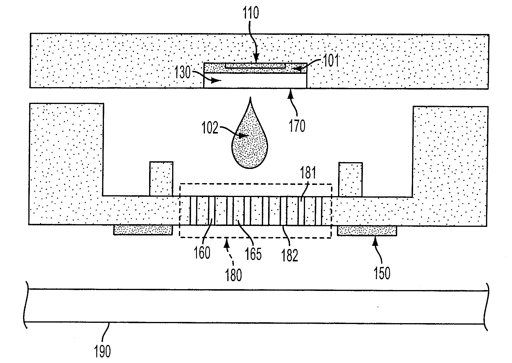
[0041]In one embodiment, the disclosure relates to a method and apparatus for depositing a film in substantially solid form on a substrate. Such films can be used, for example, in the design and construction of OLEDs and large area transistor circuits. In one embodiment, the disclosure relates to a method and apparatus for depositing a film of material in substantially solid form on a substrate. In another embodiment, the disclosure relates to a method and apparatus for depositing a film of material substantially free of solvent of a substrate. Such films can be used, for example, in the design and construction of OLEDs and large area transistor circuits. The materials that may be deposited by the apparatuses and methods described herein include organic materials, metal materials, and inorganic semiconductors and insulators, such as inorganic oxides, chalcogenides, Group IV semiconductors, Group III-V compound semiconductors, and Group II-VI semiconductors.

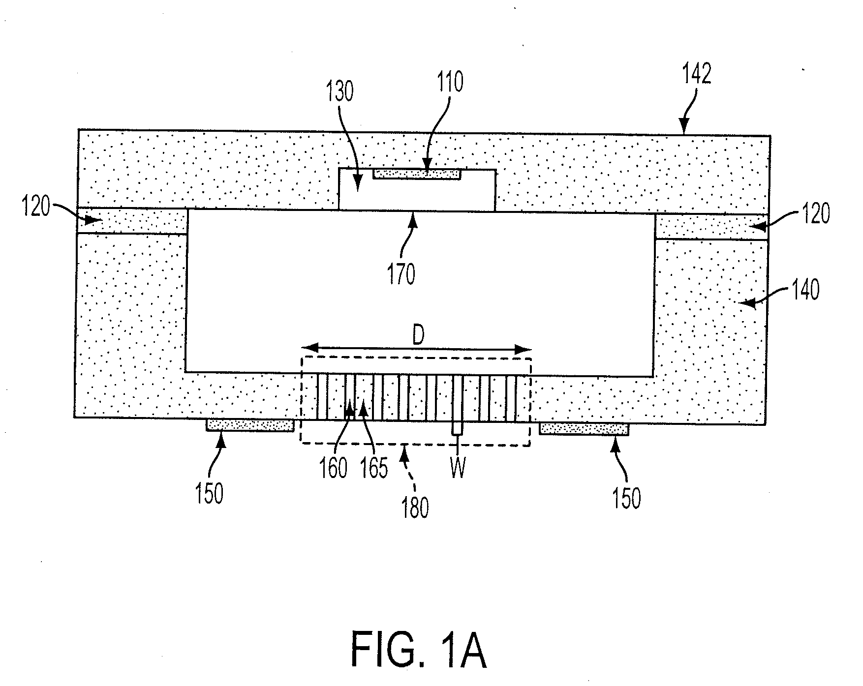
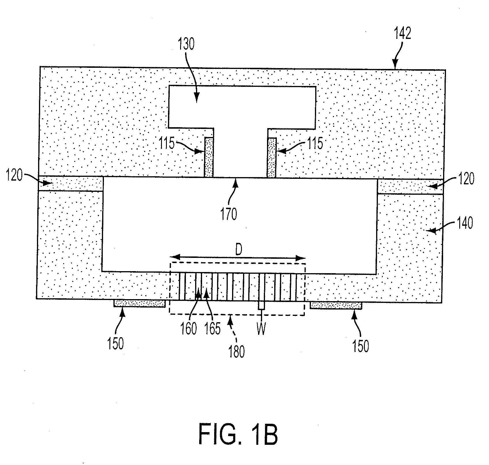
[0042]FIG. 1A is a schemat...


PUM


Abstract

The disclosure relates to a method for depositing films on a substrate which may form part of an LED or other types of display. In one embodiment, the disclosure relates to an apparatus for depositing ink on a substrate. The apparatus includes a chamber for receiving ink; a discharge nozzle having an inlet port and an outlet port, the discharge nozzle receiving a quantity of ink from the chamber at the inlet port and dispensing the quantity of ink from the outlet port; and a dispenser for metering the quantity of ink from the chamber to the inlet port of the discharge nozzle; wherein the chamber receives ink in liquid form having a plurality of suspended particles and the quantity of ink is pulsatingly metered from the chamber to the discharge nozzle; and the discharge nozzle evaporates the carrier liquid and deposits the solid particles on the substrate.

Description

[0001]The instant application claims priority to Provisional Application No. 60 / 944,000 entitled “METHOD AND APPARATUS FOR DEPOSITING FILMS,” filed Jun. 14, 2007, which is hereby incorporated herein by reference in its entirety.BACKGROUND[0002]1. Field of the Invention[0003]The disclosure relates to a method and apparatus for efficiently depositing patterns of films on a substrate. More specifically, the disclosure relates to a method and apparatus for depositing films on a substrate which may form part of an LED or other types of display.[0004]2. Description of Related Art[0005]The manufacture of organic light emitting devices (OLEDs) requires depositing one or more organic films on a substrate and coupling the top and bottom of the film stack to electrodes. The film thickness is a prime consideration. The total layer stack thickness is about 100 nm and each layer is optimally deposited uniformly with an accuracy of better than ±1 nm. Film purity is also important. Conventional app...

Claims


Application Information

Patent Timeline
IPC IPC(8): B05B7/16
CPCB05B17/0638B41J2/14B41J2202/09B41J2202/16B41J2/04588H01L51/56B41J2/07H05B33/10B41J2/04581H01L51/0005H10K71/135H10K71/00B41J2/32B41J2/175B41J2/045
Inventor BULOVIC, VLADIMIRCHEN, JIANGLONGMADIGAN, CONOR FRANCISSCHMIDT, MARTIN A.
Owner MASSACHUSETTS INST OF TECH
Why Eureka
Try Eureka