Under such circumstances, the reliability of a gate dielectric layer is now regarded as more of an important issue than ever before.
As a result, the
gate oxide layer looses the electrical insulating properties, causing the gate and the channel region to be electrically shorted, which, in turn, leads to the failure of a MOSFET.
This process creates numerous defects (energy traps) in the
oxide layer.
Extrinsic breakdown are breakdown events attributable to defects brought into the
oxide during manufacturing processes.
These defects may include oxide roughness, particles in oxide, etc.
This process ultimately leads to device breakdown as a conductive path is formed between the gate
electrode and the substrate.
In practice, reliability testing on a
gate oxide is usually carried out in an “accelerated” manner where excess stress (voltage and / or current) is applied on the
gate oxide to accelerate the breakdown process since reliability testing under operating conditions will take an impractically long period of time.
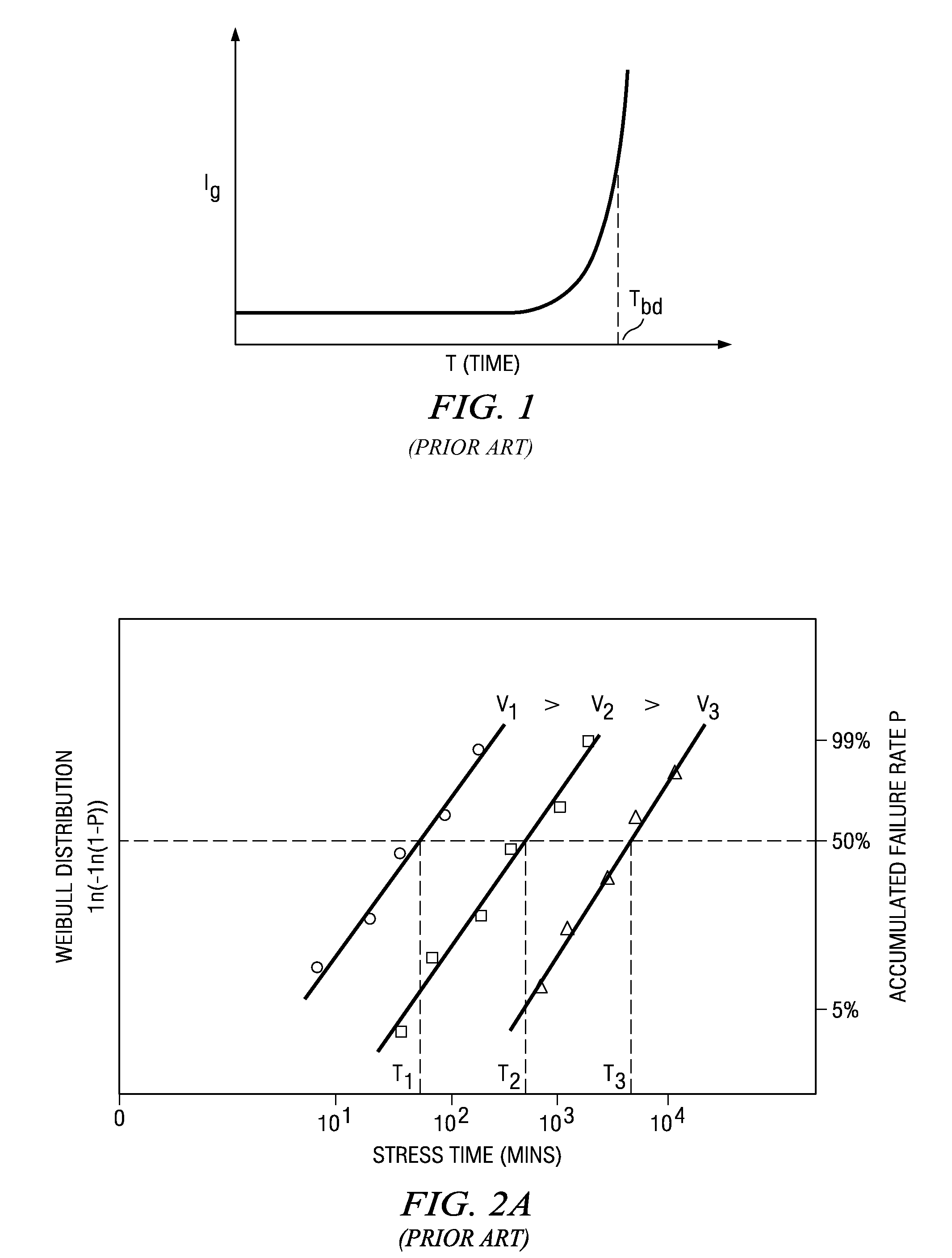
Under high stresses of a burn-in test, the oxide accumulates defects faster and a device fails more quickly.
Under such stress application, oxide
layers of each group experience a time dependent dielectric breakdown and the number of failed oxide
layers increases with the passage of time.
First, a process condition change, in particular, changes relating to steps of forming a gate in a MOSFET will most likely change the quality of a gate oxide layer.
Even though burn-in testing is employed to “accelerate”
device failure, prior art test methods, such as the
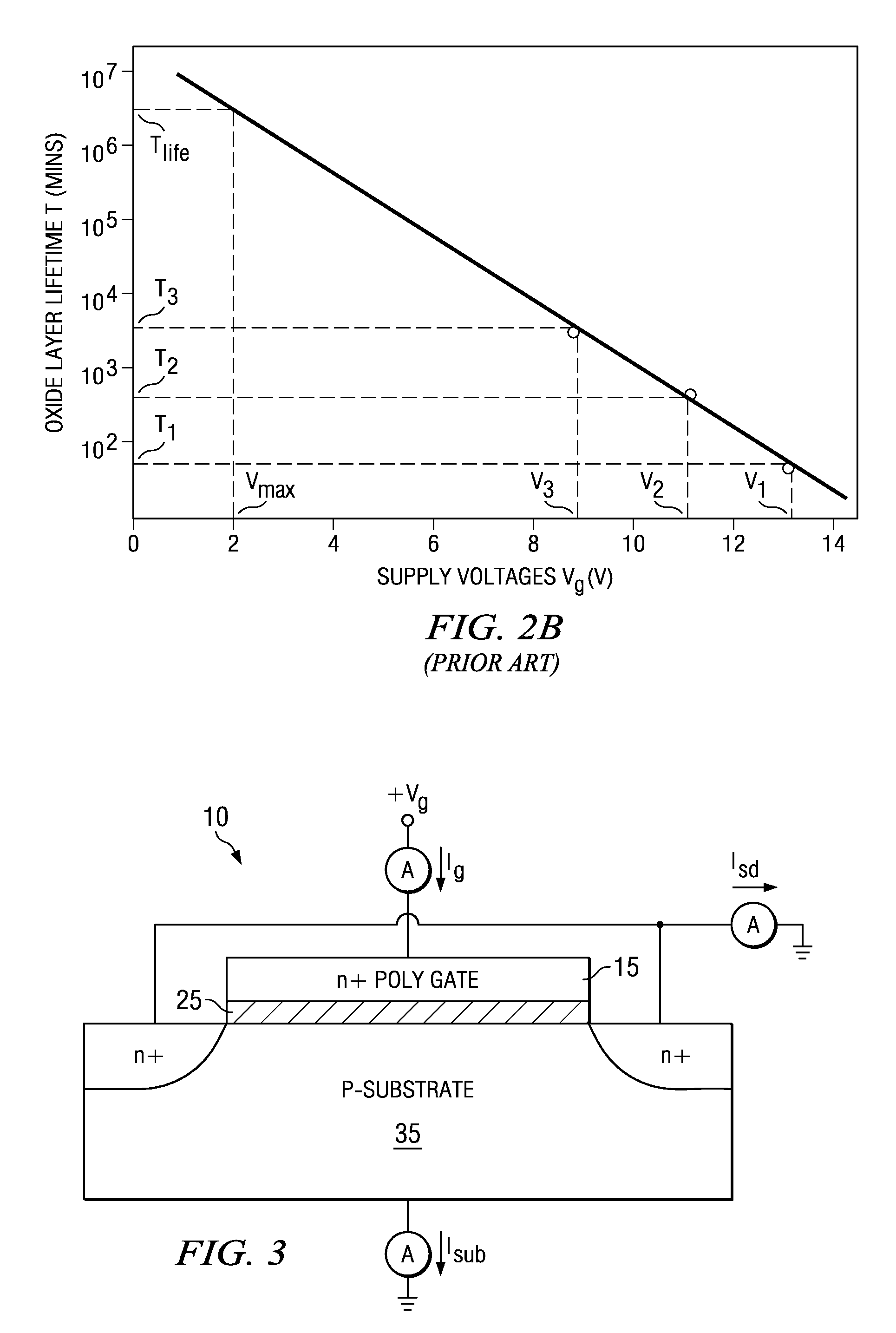
constant voltage method described in above example, still last for days or even weeks to obtain the voltage
acceleration factor and estimated oxide layer lifetime.
Due to this hindrance, in practice, TDDB tests are only conducted under a few stress voltages on a limited number of samples out of a manufactured batch.
These limitations lead to poor statistics on test results.
This drastically increases the errors in the voltage
acceleration factor and estimated oxide layer lifetime.
Unfortunately, this assumption is very rough and produces large errors in the extraction of voltage acceleration factors and oxide layer lifetime
estimation.
As an example, the high
electric field in an oxide layer under
high stress voltages generates a large amount of heat, which causes the oxide layer to increase in temperature.
This leads to a shorter time period between the application of stress voltages and the time dependent dielectric breakdown (TDDB) of the oxide layer, when compared to the oxide layer breakdown time period with the use of normal temperatures and operating voltages.
On occasion, an
estimation error can be as large as years.
This problem can also lead to a major
impact on the cost of a
semiconductor device manufacturing facility, where devices with good reliability can be unfavorably downgraded or scrapped due to the overly conservative
estimation on oxide layer lifetime from a burn-in test.

