Circuit, biasing scheme and fabrication method for diode accesed cross-point resistive memory array

a resistive memory array and diode access technology, applied in semiconductor devices, digital storage, instruments, etc., can solve the problems of large power consumption, devices unsuitable for portable devices or as substitutes for frequently-accessed volatile memory devices, and significant power consumption

Active Publication Date: 2008-12-18
MICRON TECH INC
View PDF19 Cites 17 Cited by
  • Summary
  • Abstract
  • Description
  • Claims
  • Application Information

AI Technical Summary

Problems solved by technology

Traditionally, however, non-volatile memory devices occupy a large amount of space and consume large quantities of power, making these devices unsuitable for use in portable devices or as substitutes for frequently-accessed volatile memory devices.
However, volatile memory devices require a continuous power supply in order to retain stored memory content.
Considering the large number of reverse biased diodes in the array 50, the resulting standby current results in significant power consumption.

Method used


Image

  • Circuit, biasing scheme and fabrication method for diode accesed cross-point resistive memory array
  • Circuit, biasing scheme and fabrication method for diode accesed cross-point resistive memory array
  • Circuit, biasing scheme and fabrication method for diode accesed cross-point resistive memory array

Examples


Embodiment Construction

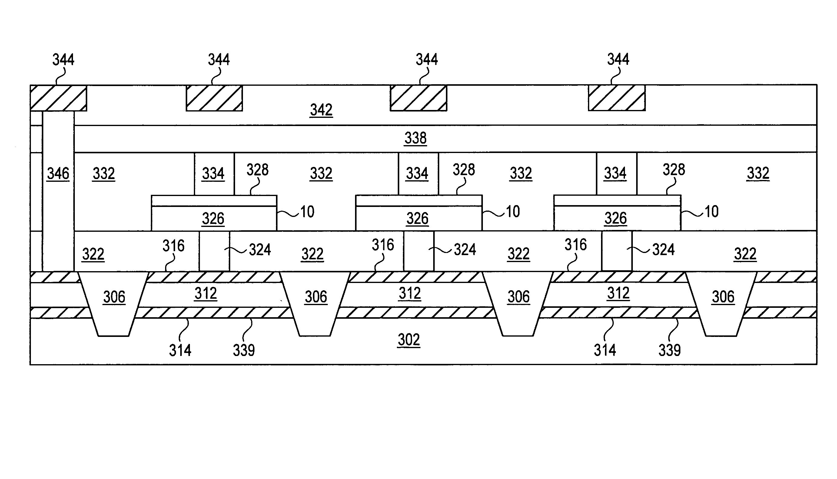
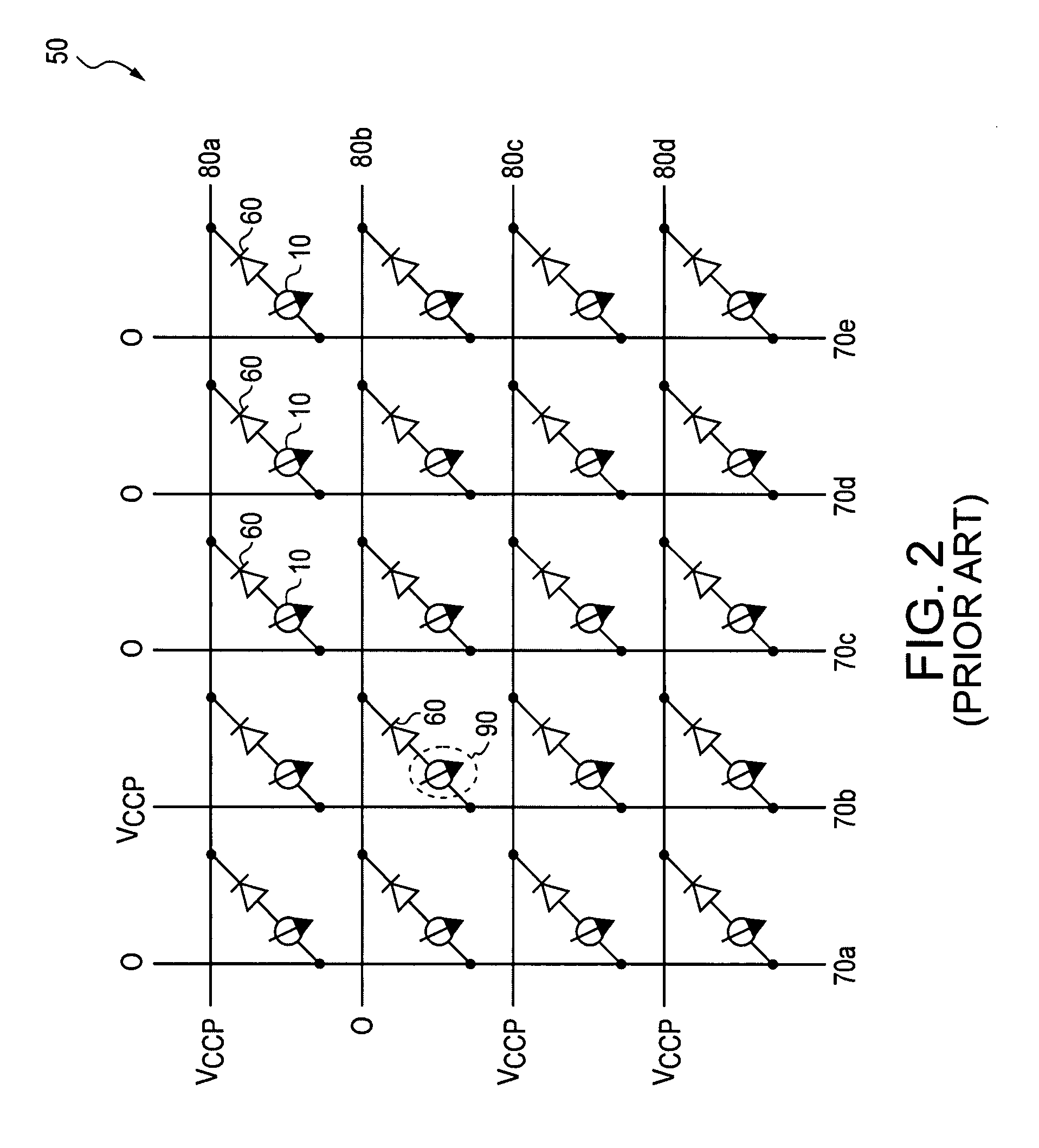
[0020]In order to, for example, reduce standby power consumption and / or operational delays in a diode accessed cross-point resistive memory array, back-to-back Zener diodes may be used instead of the single diode used in the prior art. A Zener diode has a current-voltage (i.e., I-V) chart 102 as shown in FIG. 3. In the I-V chart 102, current is represented on the vertical axis. Voltage is represented on the horizontal axis. When a Zener diode is positively biased (i.e., when the voltage is positive in the I-V chart 102), a Zener diode acts like a typical bipolar diode. However, when a Zener diode is reverse biased (i.e., the applied voltage is negative in the I-V chart 102), very little leakage current flows and the Zener diode acts effectively as an open circuit as long as the magnitude of the reverse bias is less than the Zener voltage VZ. When the reverse bias is increased to the Zener voltage VZ, the Zener diode breaks down and a dramatic increase in current occurs. The increase...


PUM


Abstract

Methods, systems, structures and arrays are disclosed, such as a resistive memory array which includes access devices, for example, back-to-back Zener diodes, that only allow current to pass through a coupled resistive memory cell when a voltage drop applied to the access device is greater than a critical voltage. The array may be biased to reduce standby currents and improve delay times between programming and read operations.

Description

FIELD OF THE INVENTION[0001]The embodiments of the invention relate generally to the field of semiconductor devices and, more particularly, to resistive memory devices, e.g., phase change memory devices.BACKGROUND OF THE INVENTION[0002]Microprocessor-accessible memory devices have traditionally been classified as either non-volatile or volatile memory devices. Non-volatile memory devices are capable of retaining stored information even when power to the memory device is turned off. Traditionally, however, non-volatile memory devices occupy a large amount of space and consume large quantities of power, making these devices unsuitable for use in portable devices or as substitutes for frequently-accessed volatile memory devices. On the other hand, volatile memory devices tend to provide greater storage capability and programming options than non-volatile memory devices. Volatile memory devices also generally consume less power than non-volatile devices. However, volatile memory devices...

Claims


Application Information

Patent Timeline
Patent Type & Authority Applications(United States)
IPC IPC(8): G11C11/00G11C5/14H01L21/8234
CPCG11C13/0004G11C13/003G11C2213/71G11C2213/72G11C2213/74H01L27/2463H01L45/06H01L45/1233H01L45/144H01L27/2409G11C2213/76H10B63/20H10B63/80H10N70/231H10N70/8828H10N70/826
Inventor LIU, JUNPORTER, DAVID
Owner MICRON TECH INC
Why Eureka
Try Eureka