Trenched MOSFETs with improved gate-drain (GD) clamp diodes

a technology of gate-drain diodes and mosfets, which is applied in the field of cell structures, device configuration and fabrication processes of power semiconductor devices, can solve the problems of circuits and methods still having disadvantages and limitations, and the suitable mosfet device of conventional technologies still has avalanche protection and other problems, to achieve the effect of preventing a channeling

Active Publication Date: 2008-10-23
FORCE MOS TECH CO LTD
View PDF20 Cites 49 Cited by
  • Summary
  • Abstract
  • Description
  • Claims
  • Application Information

AI Technical Summary

Benefits of technology

[0009]Briefly, in a preferred embodiment, the present invention discloses a MOSFET device that includes a first Zener diode connected between a gate metal and a drain metal of said semiconductor power device for functioning as a gate-drain (GD) clamp diode. The GD clamp diode includes multiple back-to-back doped regions in a polysilicon layer doped with dopant ions of a first conductivity type next to a second conductivity type disposed on an insulation layer above the MOSFET device, having an avalanche voltage lower than a source / drain avalanche voltage of the MOSFET device wherein the Zener diode is insulated from a doped region of the MOSFET device for preventing a channeling effect. The MOSFET device further includes a second Zener diode connected between a gate metal and a source metal of the MOSFET device for functioning as a gate-source (GS) clamp diode, wherein the GD clamp diode includes multiple back-to-back doped regions in the polysilicon layer doped with dopant ions of a first conductivity type next to a second conductivity type disposed on the insulation layer above the MOSFET device having a lower breakdown voltage than a gate oxide rupture voltage of the MOSFET device. The MOSFET device further includes a gate-connection doped region in the polysilicon layer disposed between and connected to the GD clap diode and the GS diode wherein the gate-connection doped region further connected to the gate metal. In an exemplary embodiment, the MOSFET device includes a N-channel metal oxide semiconductor field effect transistor (MOSFET) device and the GD clamp diode and the GS claim diode includes multiple back-to-back doped regions with a polysilicon layer doped with N+ dopant ions next to a P dopant ions disposed on an insulation layer above the MOSFET device. In another exemplary embodiment, the MOSFET device further includes an preservation layer having a thickness substantially greater than five hundred (500) Angstroms for supporting and insulating the GD clamp diode and the GS clamp diode from the semiconductor power device. In another exemplary embodiment, the MOSFET device further includes a gate-connection doped region in said polysilicon layer disposed between and connected to said GD clap diode and said GS diode comprising a N+ doped region in said polysilicon layer for connecting to said gate metal.

Problems solved by technology

Conventional technologies still have technical difficulties in providing effective avalanche protection for the semiconductor power devices.
But these circuits and methods still have their disadvantages and limitations.
The G-D clamp diodes however are built as part of the floating ring structure and such structure is not suitable of MOSFET device implemented with the field plate in the termination area.

Method used


Image

  • Trenched MOSFETs with improved gate-drain (GD) clamp diodes
  • Trenched MOSFETs with improved gate-drain (GD) clamp diodes
  • Trenched MOSFETs with improved gate-drain (GD) clamp diodes

Examples


Embodiment Construction

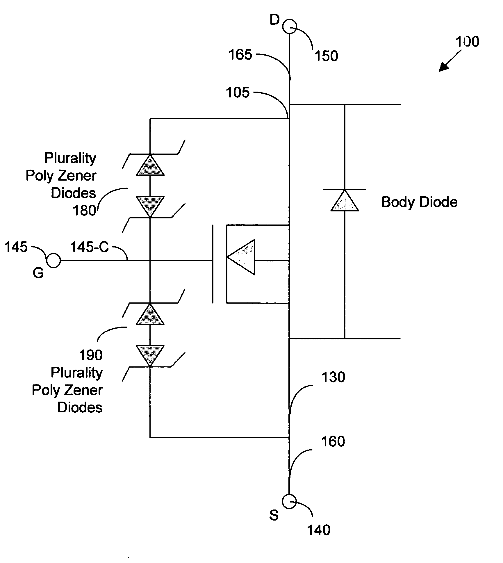
[0016]Please refer to FIGS. 2A to 2B for a circuit diagram and a side cross sectional view respectively of a first preferred embodiment of this invention. FIGS. 2A and 2B show a trenched metal oxide semiconductor field effect transistor (MOSFET) device 100 implemented with gate-drain polysilicon Zener clamp diodes 180 and gate-source polysilicon Zener clamp diodes 190 for gate-drain (GD) and gate-source (GS) protections. The trenched MOSFET 100 is supported on a substrate 105 formed with an epitaxial layer 110. The MOSFET device 100 includes a trenched gate 120 disposed in a trench with a gate insulation layer 115 formed over the walls of the trench. A body region 125 that is doped with a dopant of second conductivity type, e.g., P-type dopant, extends between the trenched gates 120. The P-body regions 125 encompassing a source region 130 doped with the dopant of first conductivity, e.g., N+ dopant. The source regions 130 are formed near the top surface of the epitaxial layer surrou...


PUM


Abstract

A MOSFET device that includes a first Zener diode connected between a gate metal and a drain metal of said semiconductor power device for functioning as a gate-drain (GD) clamp diode. The GD clamp diode includes multiple back-to-back doped regions in a polysilicon layer doped with dopant ions of a first conductivity type next to a second conductivity type disposed on an insulation layer above the MOSFET device, having an avalanche voltage lower than a source/drain avalanche voltage of the MOSFET device wherein the Zener diode is insulated from a doped region of the MOSFET device for preventing a channeling effect. The MOSFET device further includes a second Zener diode connected between a gate metal and a source metal of the MOSFET device for functioning as a gate-source (GS) clamp diode, wherein the GD clamp diode includes multiple back-to-back doped regions in the polysilicon layer doped with dopant ions of a first conductivity type next to a second conductivity type disposed on the insulation layer above the MOSFET device having a lower breakdown voltage than a gate oxide rupture voltage of the MOSFET device.

Description

BACKGROUND OF THE INVENTION[0001]1. Field of the Invention[0002]This invention relates generally to the cell structure, device configuration and fabrication process of power semiconductor devices. More particularly, this invention relates to a novel and improved cell configuration and processes to manufacture MOSFET device with an improved drain-gate clamping diode for avalanche protection by providing the GD clamp diode with lower avalanche breakdown voltage than the trenched MOSFET.[0003]2. Description of the Related Art[0004]Conventional technologies still have technical difficulties in providing effective avalanche protection for the semiconductor power devices. Several circuit structures by implementing Zener diodes for clamping the gate-source and gate-drain voltage for avalanche protection are disclosed. But these circuits and methods still have their disadvantages and limitations.[0005]In U.S. Pat. No. 5,079,608 a the lateral N+ / P Zener diodes disposed between the gate and d...

Claims


Application Information

Patent Timeline
Patent Type & Authority Applications(United States)
IPC IPC(8): H01L27/06H01L21/8234
CPCH01L27/0255H01L27/0629H01L27/0814
Inventor HSHIEH, FWU-IUAN
Owner FORCE MOS TECH CO LTD
Why Eureka
Try Eureka