In-situ high-resolution light-optical channel for optical viewing and surface processing in parallel with charged particle (fib and sem) techniques

a high-resolution, surface processing technology, applied in the field of focused ion beam tools, can solve problems such as fib processing, and achieve the effect of uniform removal rate and avoiding ion channeling effects

Inactive Publication Date: 2008-11-20
GLOBALFOUNDRIES INC
View PDF13 Cites 12 Cited by
  • Summary
  • Abstract
  • Description
  • Claims
  • Application Information

AI Technical Summary

Benefits of technology

[0006]The problems related to FIB processing arise because the gallium ion beam is the sole source of activating energy. Some of these problems could be overcome if, in addition to the energy provided by the FIB ion beam, one could introduce light energy to the surface. For example, a high-resolution optical microscope would allow non-destructive and non-staining optical viewing and navigation white FIB processing is being performed. Photo-induced chemical reactions for removing or depositing materials could also be exploited without exposing the surface to the ion beam. Alternatively, in conjunction with beam energy, possible unique reaction dynamics may be created. For instance, impact sputtering could slowly expose new surfaces, while the photon induced chemistry converts the surface. As an example, light and oxygen might convert a polycrystalline material into an amorphous oxide, and the ion beam sputters it away. The result would be a potentially more uniform removal rate, that avoids ion channeling effects.
[0008]It is another object of the present invention to enable in an FIB tool the ability to make photochemical reactions to be made on the surface of an electronic device by delivering high-intensity light to the surface of the device.

Problems solved by technology

The problems related to FIB processing arise because the gallium ion beam is the sole source of activating energy.

Method used


Image

  • In-situ high-resolution light-optical channel for optical viewing and surface processing in parallel with charged particle (fib and sem) techniques
  • In-situ high-resolution light-optical channel for optical viewing and surface processing in parallel with charged particle (fib and sem) techniques
  • In-situ high-resolution light-optical channel for optical viewing and surface processing in parallel with charged particle (fib and sem) techniques

Examples


Embodiment Construction

)

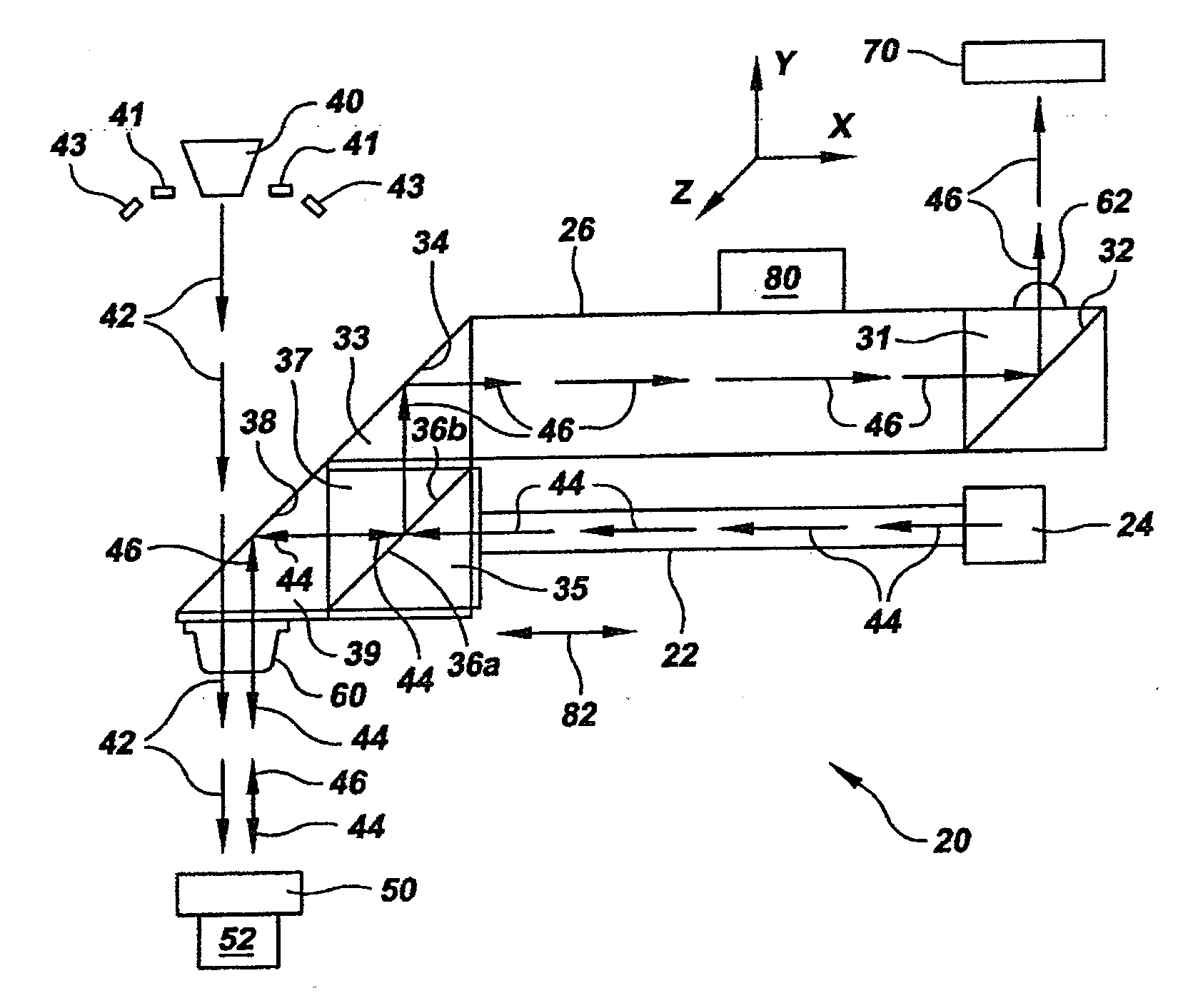
[0030]In describing the preferred embodiment of the present invention, reference will be made herein to FIGS. 1-7 of the drawings in which like numerals refer to like features of the invention.

[0031]FIG. 1 illustrates in schematic view a preferred embodiment of the optical channel viewing and processing device of the present invention. A sample 50, such as an electronic device or other object, is mounted on a stage 52 movable in the x-, y- and z-directions. An otherwise conventional focused ion beam (FIB) tool comprises an ion beam source 40 that generates ion beam 42 that strikes the upper surface of sample 50, generating secondary electrons and secondary ions (not shown). A microchannel plate or other charged particle detector 41 is disposed azimuthally about the ion beam 42. Detector 41 is either positively biased to attract secondary electrons in the electron mode, or negatively biased to attract secondary ions in the ion mode. A conversion dynode 43 azimuthally positioned abou...


PUM


Abstract

An apparatus for simultaneous parallel processing of a sample using light energy for optical viewing or surface processing in parallel with a charged particle beam. A charged particle beam transmits a focused ion beam or an electron beam along a path to a sample. An optical microscope transmits light along a first path to the sample, and a prism aligned along the first light path reflects light into a second light path toward the sample. A portion of the prism and reflective surface is removed for passage of the charged particle beam. A lens is aligned along the second light path and has a portion removed for passage of the charged particle beam. The removed portions of the prism and lens are aligned along the charged particle beam path to permit parallel delivery of the charged particle beam and the light to substantially the same portion of the sample.

Description

BACKGROUND OF THE INVENTION[0001]1. Field of the Invention[0002]The present invention relates to focused ion beam tools and in particular to a system and method of permitting optical viewing and surface processing of semiconductor wafers and associated devices in parallel with ion beam processing of those wafers.[0003]2. Description of Related Art[0004]Focused ion beam (FIB) toots are widely used in processing of semiconductor wafers and associated devices (collectively referred to as electronic devices), particularly in circuit editing, failure analysis (FA) and mask repair applications. FIB tools have the ability to sputter away or deposit materials over selected microscopic areas. Though FIB tools are useful and powerful, they have limitations towards some applications. In circuit editing, for example, copper features are difficult to sputter cleanly with an ion beam, and new low dielectric constant (low-k) materials can be damaged by the FIB tool's gallium ion beam. In mask repa...

Claims


Application Information

Patent Timeline
Patent Type & Authority Applications(United States)
IPC IPC(8): G21K5/00
CPCH01J37/228H01J37/304H01J37/3056H01J2237/28H01J2237/31742H01J2237/31749
Inventor HERSCHBEIN, STEVEN B.MARCHMAN, HERSCHEL M.RANA, NARENDERRUE, CHAD
Owner GLOBALFOUNDRIES INC
Why Eureka
Try Eureka