Light-emitting semiconductor device having an overvoltage protector, and method of fabrication

a technology of overvoltage protector and light-emitting semiconductor, which is applied in the direction of emergency protective circuit arrangement, emergency protective arrangement for limiting excess voltage/current, solid-state device, etc., can solve the problems of unnecessarily bulky, complex and costly construction of overvoltage-proof light-emitting device, and device susceptible to breakdown, etc. , to achieve the effect of less expensive construction, simple structure and less bulky

Inactive Publication Date: 2006-03-16
SANKEN ELECTRIC CO LTD
View PDF7 Cites 53 Cited by
  • Summary
  • Abstract
  • Description
  • Claims
  • Application Information

AI Technical Summary

Benefits of technology

[0005] The present invention seeks to combine a light-emitting semiconductor device and an overvoltage protector therefor into an integrated semiconductor device of simpler, more compact and less expensive construction than heretofore.

Problems solved by technology

These devices were therefore susceptible to breakdown from overvoltages due to static electricity.
This known solution is objectionable because of the need for fabrication of the flip-chip light-emitting device and the overvoltage protector independently of each other.
Such loose integration of the two functional components made the overvoltage-proof light-emitting device unnecessarily bulky in size and complex and costly in construction.

Method used


Image

  • Light-emitting semiconductor device having an overvoltage protector, and method of fabrication
  • Light-emitting semiconductor device having an overvoltage protector, and method of fabrication
  • Light-emitting semiconductor device having an overvoltage protector, and method of fabrication

Examples


embodiment

OF FIG. 5

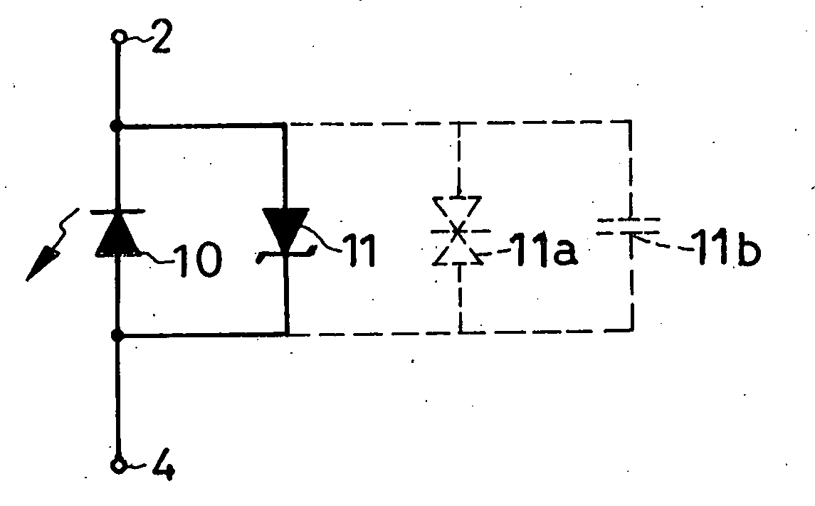
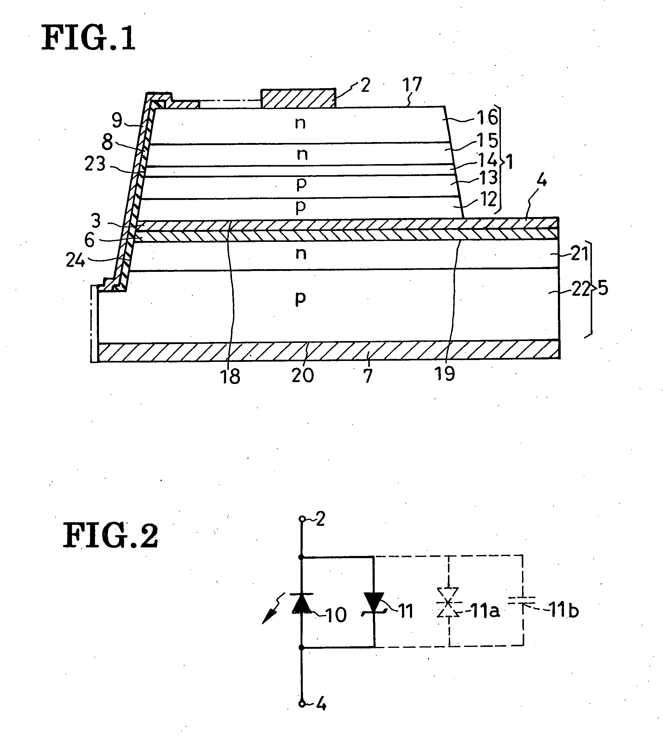
[0071]FIG. 5 shows the second preferred form of overvoltage-protected light-emitting device according to the invention, which is akin in construction to the first preferred form of FIG. 1 except that a different method is employed here for electrically interconnecting the LED and zener diode. The FIG. 5 device has a channel 30 extending centrally therethrough between the major surface 17 of the light-emitting semiconductor region 1 and the major surface 20 of the protector baseplate 5. The channel 30 is in register with the first electrode 2 and less in cross sectional size than the same, so that it does not interfere with light emission by the device.

[0072] Received in the channel 30 are a tubular insulator 8a and, within it, a connector 9a. The insulator 8a is directly held against the surfaces bounding the channel 30. The connector 9a has a pair of opposite ends both projecting from within the insulator 8a and both flanged. One flanged end of the connector 9a is held ag...


PUM


Abstract

An LED includes a light-generating semiconductor region having an active layer sandwiched between two confining layers of opposite conductivity types for generating light. A cathode is arranged centrally on one of the opposite major surfaces of the semiconductor region from which is emitted the light. A reflector of electroconductive material is formed on the other major surface of the semiconductor region for reflecting the light back toward the light-emitting surface of the semiconductor region. For protecting the LED against breakdown from overvoltages, a zener diode is employed which takes the form of a baseplate having two semiconductor regions of opposite conductivity types sandwiched between a pair of electrodes in the form of metal layers. The protector baseplate is integrated with the light-generating semiconductor region by joining one of the metal layers to the reflector under heat and pressure, thus serving as both mechanical support and overvoltage protector for the LED.

Description

CROSS REFERNCE TO RELATED APPLICATIONS [0001] This application claims priority to Japanese Patent Application No. 2004-268792, filed Sep. 15, 2004. BACKGROUND OF THE INVENTION [0002] This invention relates to light-emitting semiconductor devices, or light-emitting diodes (LEDs) according to common parlance, which find use in lamps, displays and so forth. More particularly, the invention pertains to light-emitting semiconductor devices made from nitrides and other Groups III-V compound semiconductors, and, still more particularly, to those incorporating an overvoltage protector for saving them from electrical breakdown due to voltage surges. The invention also deals with a method of making such overvoltage-protected light-emitting semiconductor devices. [0003] Light-emitting semiconductor devices made from nitrides and other Groups III-V compound semiconductors are capable of withstanding voltage surges only up to 100 volts or so. These devices were therefore susceptible to breakdown...

Claims


Application Information

Patent Timeline
Patent Type & Authority Applications(United States)
IPC IPC(8): H02H9/00H01L33/10H01L33/14H01L33/32H01L33/34H01L33/40
CPCH01L25/167H01L27/15H01L2924/01029H01L2224/48464H01L2924/01012H01L24/48H01L2924/00014H01L2924/12035H01L2924/12036H01L2224/45099H01L2924/00H01L2224/85399H01L2224/05599
Inventor AOYAGI, HIDEKAZUMATSUO, TETSUJI
Owner SANKEN ELECTRIC CO LTD
Why Eureka
Try Eureka