Plasmon resonance sensor

a technology of plasmon resonance and sensor, applied in the direction of material analysis through optical means, scattering properties measurement, measurement devices, etc., can solve the problem of obviating comparatively expensive optical components, and achieve the effect of reducing production costs and increasing performan

Inactive Publication Date: 2011-07-05
FRAUNHOFER GESELLSCHAFT ZUR FOERDERUNG DER ANGEWANDTEN FORSCHUNG EV
View PDF10 Cites 2 Cited by
  • Summary
  • Abstract
  • Description
  • Claims
  • Application Information

AI Technical Summary

Benefits of technology

[0010]The convergent irradiation of the metal layer enables a compact design with small components or optical elements both on the light incidence side and on the light emergence side, in which case very narrow partial areas which are closely adjacent to one another can also be employed in the interests of a large number of measurement cells.
[0011]Expedient configurations and developments of the invention are apparent from the dependent claims. In this case, in particular the use of a chip composed of a light-transmissive polymeric plastic as light-transmissive body contributes to simplification and increase in performance since it can be produced inexpensively and simultaneously by corresponding shaping also with optical functions for the light guiding on the emergence side, and if appropriate also on the incidence side, by way of injection molding, as is known in principle from DE 103 24 973 B4. This affords the possibility of designing the chip as a replaceable disposable article, such that regeneration measures become superfluous and not only can a plurality of measurements be carried out simultaneously but the multiple measurements can also be performed in rapid succession. A comparatively expensive optical component is obviated as a result of the integration of the collimation lens into the chip. Furthermore, the insertion of the chip into the plasmon resonance sensor results in an optical coupling between the illumination optics and the detection optics without a disturbance-prone coupling by means of immersion media.

Problems solved by technology

A comparatively expensive optical component is obviated as a result of the integration of the collimation lens into the chip.

Method used


Image

  • Plasmon resonance sensor
  • Plasmon resonance sensor
  • Plasmon resonance sensor

Examples


Embodiment Construction

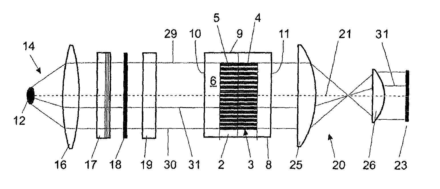
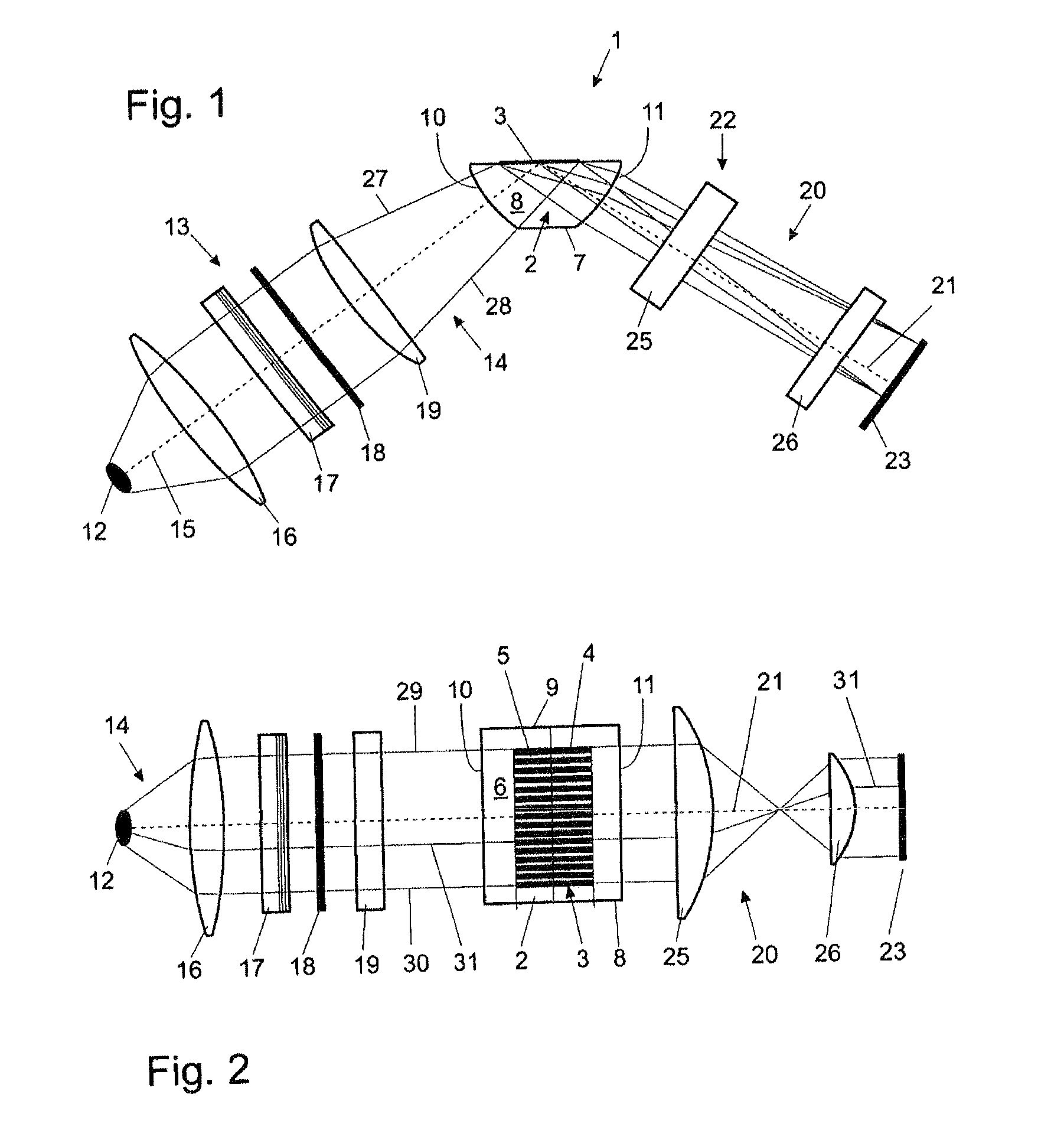
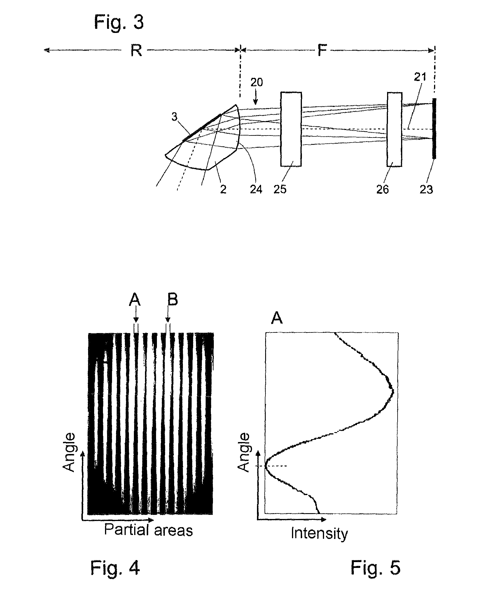
[0020]The plasmon resonance sensor 1, the essential parts of which are illustrated in FIGS. 1 and 2, has a light-transmissive body 2, which is a chip composed of a polymeric plastic and produced by injection molding. This chip 2 bears on its top side 6 a light-reflecting thin metal layer 3, which is preferably composed of gold. By means of a chemical modification of the gold surface, the latter acquires a structure wherein individual narrow partial areas 4 which are arranged closely adjacent to one another and are spaced apart by intermediate strips 5 are arranged alongside one another in a series (FIG. 2). The chip 2 has a planar top side 6 and a planar underside 7 parallel thereto, which are connected to one another by likewise planar end sides 8 and 9. By contrast, the side faces 10 and 11, as can be seen from FIGS. 1 and 3, are cylindrically curved.

[0021]The chip 2 is assigned a light source 12 and an incidence optical unit 13, whereby an incident beam path 14 with optical incid...


PUM

PropertyMeasurementUnit
radiusaaaaaaaaaa
distanceaaaaaaaaaa
areasaaaaaaaaaa

Abstract

The plasmon resonance sensor (1) comprises a chip (2) of transparent plastic with a gold layer (3) made up of narrow part surfaces (4), arranged in a row, on the inner side of which light from a planar light source (12) is convergently guided. A Fourier lens (24) integrated in the chip (2) forms the reflected angular spectrum on the detector (23), arranged at a focal separation (F) from the integrated Fourier lens (24) for temporal determination of the incident angle with a resonant intensity minimum of reflected light. An incident lens (13) brings about imaging of the planar light source (12) in the form of lines of light on the part surfaces (4), which are further imaged in the form of lines of light on the detector (23).

Description

CROSS-REFERENCE TO RELATED APPLICATION[0001]The invention described and claimed hereinbelow is also described in German Patent Application DE 10 2006 041 338.5 filed on Sep. 1, 2006. This German Patent Application, whose subject matter is incorporated here by reference, provides the basis for a claim of priority of invention under 35 U.S.C. 119(a)-(d).BACKGROUND OF THE INVENTION[0002]The invention relates to a plasmon resonance sensor, in particular for biosensor technology, comprising a light-transmissive body, a—applied to an area of the body—reflective metal layer or semiconductor layer having a surface which can be sensitized to molecules to be detected, which comprises partial areas arranged alongside one another in a series and serving for forming a respective one of a plurality of measurement cells, comprising an areal light source for producing a beam path incident on the inner side of the layer through the body, and comprising a detector, which captures the reflected emerge...

Claims


Application Information

Patent Timeline
Patent Type & Authority Patents(United States)
IPC IPC(8): G01N21/55
CPCG01N21/553G01N33/54373G01N2021/0321
Inventor HOFMANN, ANDREASDANZ, NORBERT
Owner FRAUNHOFER GESELLSCHAFT ZUR FOERDERUNG DER ANGEWANDTEN FORSCHUNG EV
Why Eureka
Try Eureka