Semiconductor laser apparatus and manufacturing method thereof

a semiconductor and laser technology, applied in semiconductor lasers, semiconductor devices, laser details, etc., can solve the problems of inability to conduct normal operation, insufficient esd countermeasures, and increased esd breakdown voltage, so as to improve the resistance to static voltage break down and high reliability

Active Publication Date: 2005-12-08
FUJIFILM BUSINESS INNOVATION CORP
View PDF21 Cites 54 Cited by
  • Summary
  • Abstract
  • Description
  • Claims
  • Application Information

AI Technical Summary

Benefits of technology

[0013] The present invention intends to address the problems in the related art, improve the resistance to static voltage break down by integrating a vertical-

Problems solved by technology

If electrostatic discharge (hereinafter referred to as ESD) should occur inside the device, since a large spike current flows instantaneously, this destroys or deteriorates the device causing a failure of not being capable of conducting normal operation.
According to the result, it is considered that ESD damage is a function of an oxidized aperture diameter or area and the ESD breakdown voltage increases as the oxidized aperture diameter increases.
However, the existent protective device for the VCSEL has the following problems.
Since the protective device is disposed separately from the light emitting device in Japanese Published Unexamined Patent Application No. 11-112026, in a case of handling the light emitting device as a single component, the ESD countermeasure is still insufficie

Method used


Image

  • Semiconductor laser apparatus and manufacturing method thereof
  • Semiconductor laser apparatus and manufacturing method thereof
  • Semiconductor laser apparatus and manufacturing method thereof

Examples


first embodiment

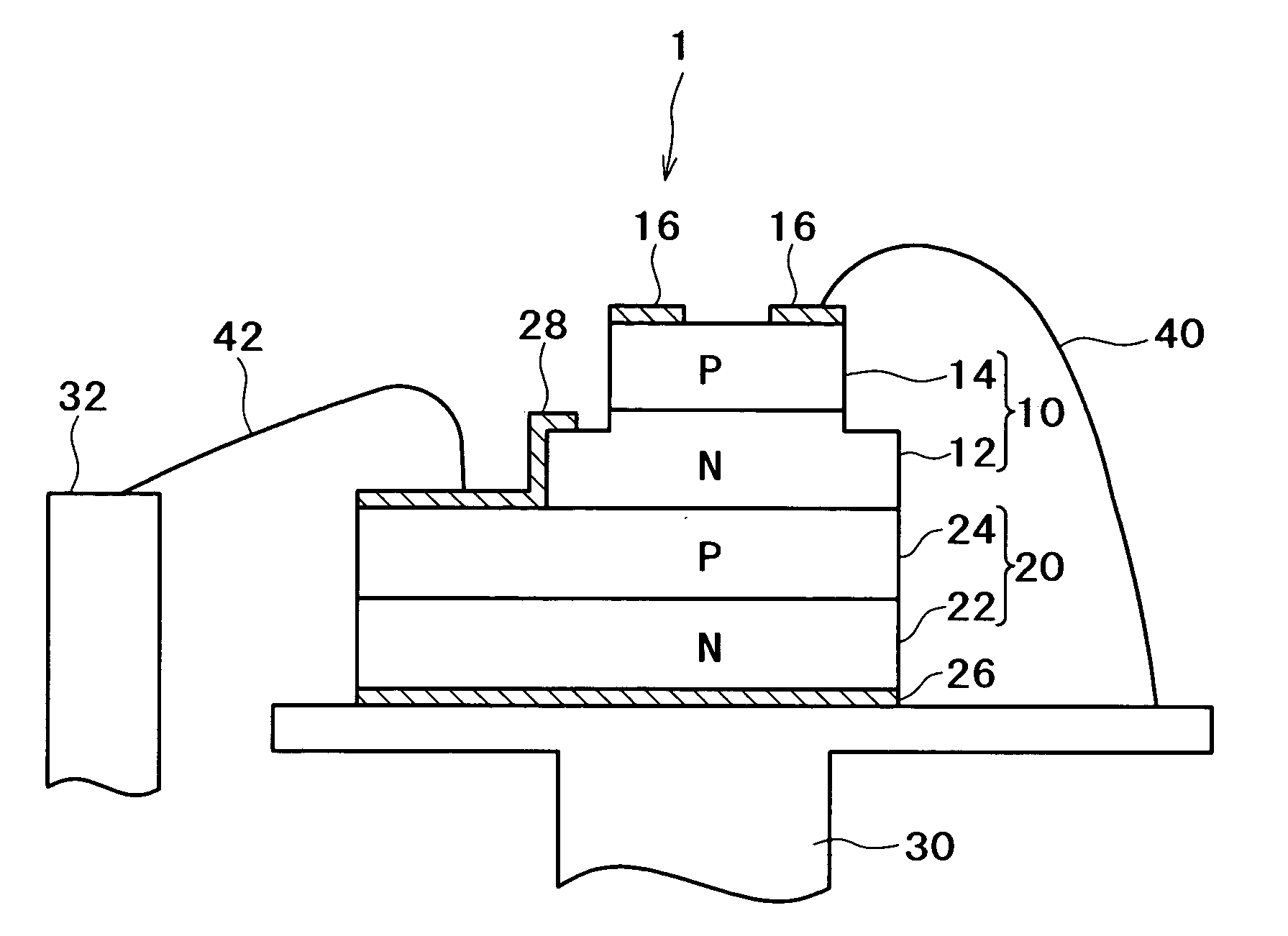
[0032]FIG. 2 is a cross sectional view showing a configuration of a semiconductor laser apparatus according to the A Zener diode contains an n-type GaAs substrate 200 and a p-type GaAs layer 210 stacked therewith. An n-side electrode layer 220 is formed at the back surface of the n-type GaAs substrate 200. For the electrode layer 220, a stack of Ti and Au can be used for instance.

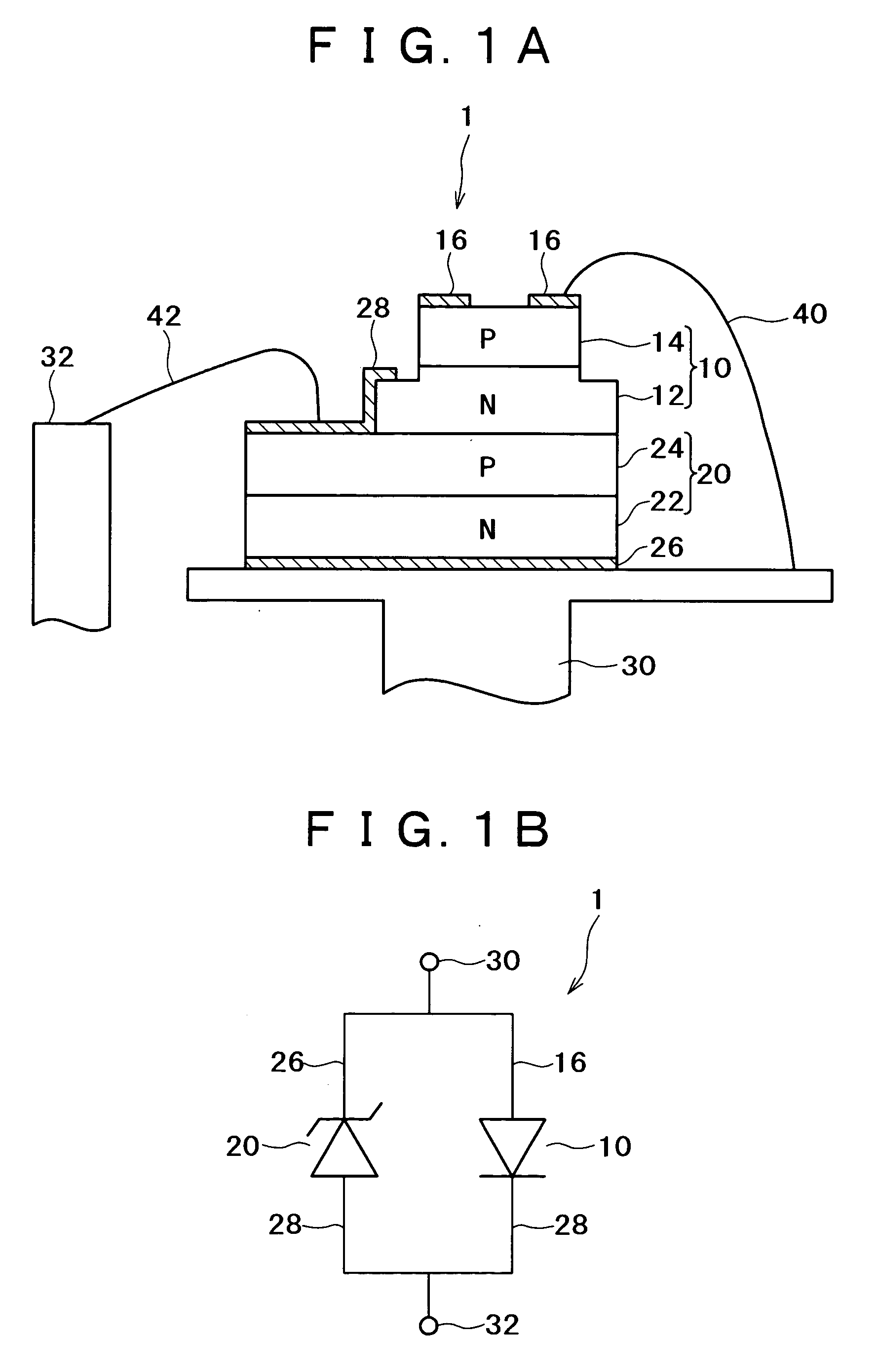
[0033] The VCSEL 10 has a first post 101 having a first diameter and a second post 102 having a second diameter larger than the first diameter of the first post. The second post is stacked above the Zener diode 20 and the first post is stacked above the second post.

[0034]“Diameter” used in this specification is defined as described below. The diameter, in a case where the post is a circular cylindrical shape, is a diameter of a cross section parallel with the substrate 200, while the diameter in a case where the post is a square cylindrical shape is an diagonal distance of a cross section parallel with th...

second embodiment

[0048] since the VCSEL 10 and the Zener diode 20 are electrically insulated from each other, it is possible to completely prevent the thyristor operation due to the PNPN structure caused by the leak current from the VCSEL 10 or the Zener diode 20.

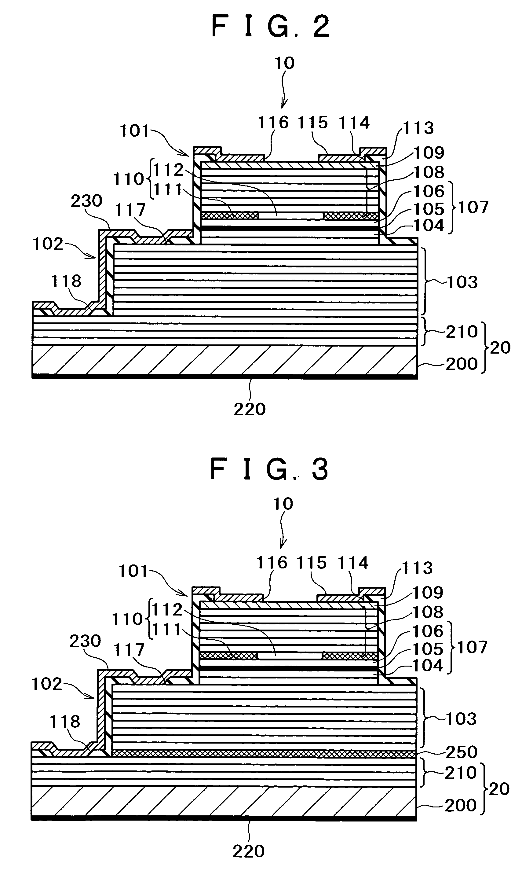
[0049]FIG. 4 is a view showing other configuration examples of Zener diodes. In the Zener diode shown in FIG. 4A, plural n-type AlGaAs layers 310, for example, are stacked above an n-type GaAs substrate 300, and p-type AlGaAs layers 320 are stacked further thereon. An n-side electrode 330 is formed at the back surface of the n-type substrate 300. The VCSEL 10 is stacked above the p-type AlGaAs layers 320 of the Zener diode. This can simply form the Zener diode and the VCSEL by epitaxial growing for once. The semiconductor layer is not limited to the AlGaAs layer and a semiconductor layer of another material may also be stacked.

[0050] Further, as shown in FIG. 4B, it may be a configuration in which a p-type GaAs substrate 340 is joined on ...


PUM


Abstract

A semiconductor laser apparatus has a Zener diode containing a first semiconductor region of a first conduction type and a second semiconductor region of a second conduction type joined with the first semiconductor region, and a vertical-cavity surface-emitting semiconductor laser diode stacked above the Zener diode and containing at least a first mirror layer of a first conduction type, a second mirror layer of a second conduction type and an active region sandwiched between the first and second mirror layers. The first semiconductor region and the second mirror layer are electrically connected and the second semiconductor region and the first mirror layer are electrically connected.

Description

BACKGROUND OF THE INVENTION [0001] 1. Field of the Invention [0002] The present invention concerns a vertical-cavity surface-emitting laser diode (hereinafter referred to as VCSEL) and, it specifically relates to a protective structure for protecting the VCSEL against electrostatic damage. [0003] 2. Description of the Related Art [0004] The VCSEL has excellent features in that it has low threshold current, small power consumption and can obtain a circular light spot easily, and light sources can be arranged as a two-dimensional array, and has been expected for use as a light source in optical communication equipment or electronic equipment. [0005] Like other semiconductor apparatuses, the VCSEL is sometimes exposed to a high voltage by static electricity curing handling of circuit substrates, etc. If electrostatic discharge (hereinafter referred to as ESD) should occur inside the device, since a large spike current flows instantaneously, this destroys or deteriorates the device caus...

Claims


Application Information

Patent Timeline
IPC IPC(8): H01S5/00H01S5/183H01S5/026H01S5/068
CPCH01S5/0261H01S5/06825H01S5/18311H01S5/18341H01S5/2009H01L2224/48091H01L2224/48247H01L2224/48257H01L2224/49107Y10S438/983Y10S438/979H01L2924/00014H01L2924/1301H01L2924/00
Inventor MURAKAMI, AKEMINAKAYAMA, HIDEOKUWATA, YASUAKISUZUKI, TEIICHIISHII, RYOJI
Owner FUJIFILM BUSINESS INNOVATION CORP
Why Eureka
Try Eureka