Direct edge connection for multi-chip integrated circuits

Inactive Publication Date: 2008-12-25
GLOBALFOUNDRIES INC
View PDF6 Cites 28 Cited by
  • Summary
  • Abstract
  • Description
  • Claims
  • Application Information

AI Technical Summary

Benefits of technology

[0006]The present invention, improves upon the prior art by providing robust multi-dimensional low contact-resistance chip-to-chip interconnections. Edge pads provid

Problems solved by technology

These aforementioned processes require many complex processing steps.
Accurate thermal modeling of the resultant layered structure is very difficult to achieve.
For example, it is unknown if heat generated at a lowest layer be adequately removed by a chip package.
If needed, signals may be routed externally through a wirebond

Method used


Image

  • Direct edge connection for multi-chip integrated circuits
  • Direct edge connection for multi-chip integrated circuits
  • Direct edge connection for multi-chip integrated circuits

Examples


Example

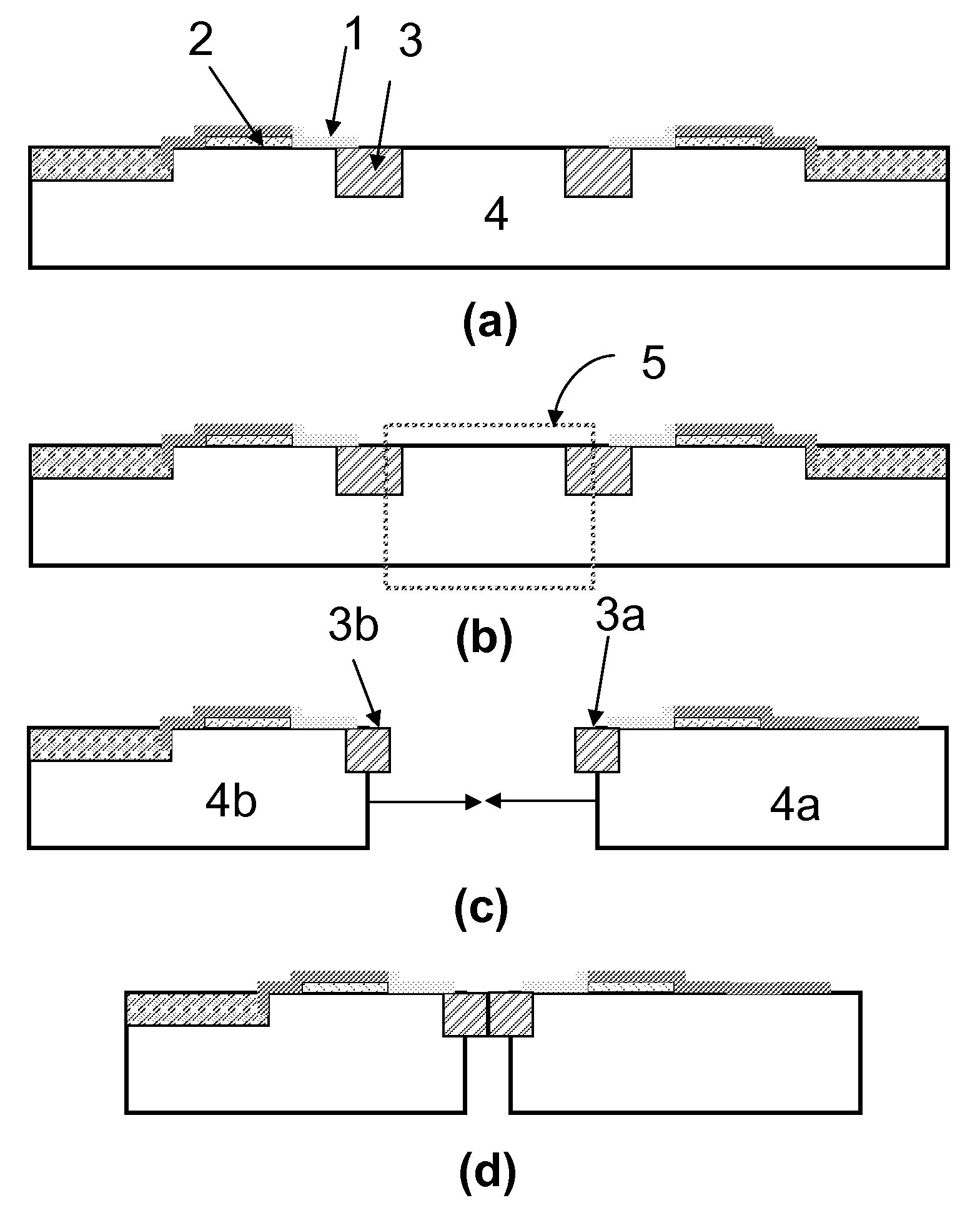
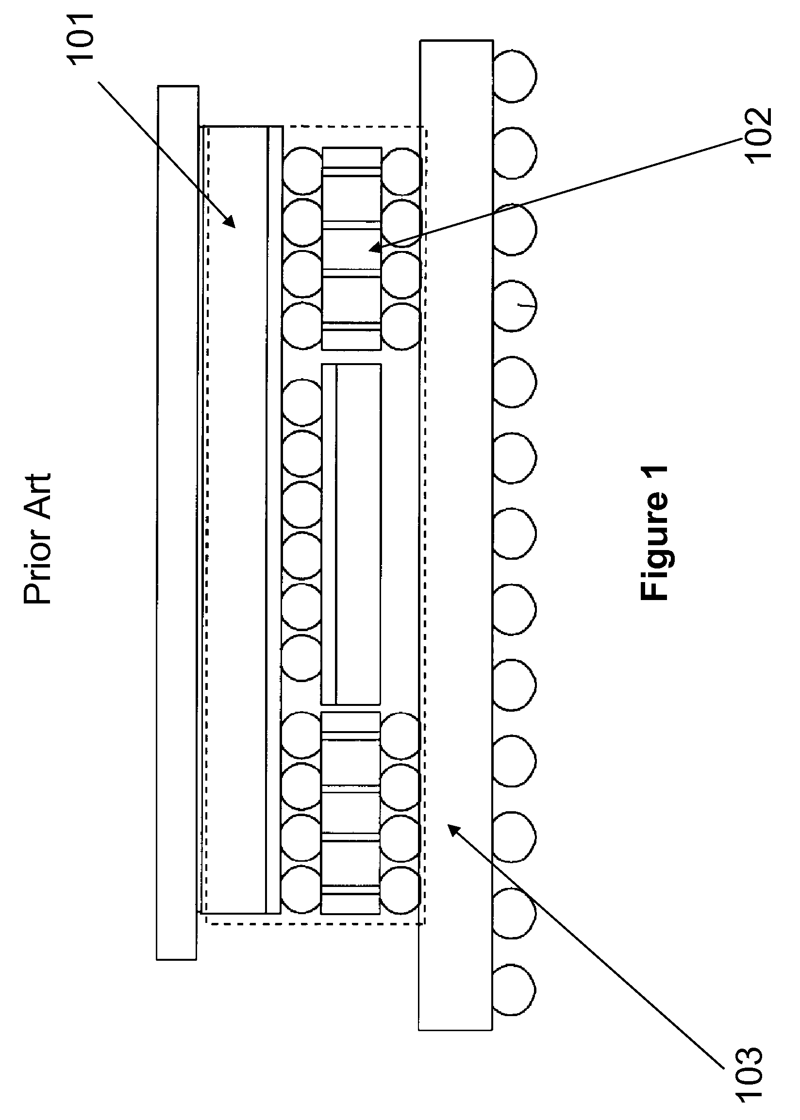
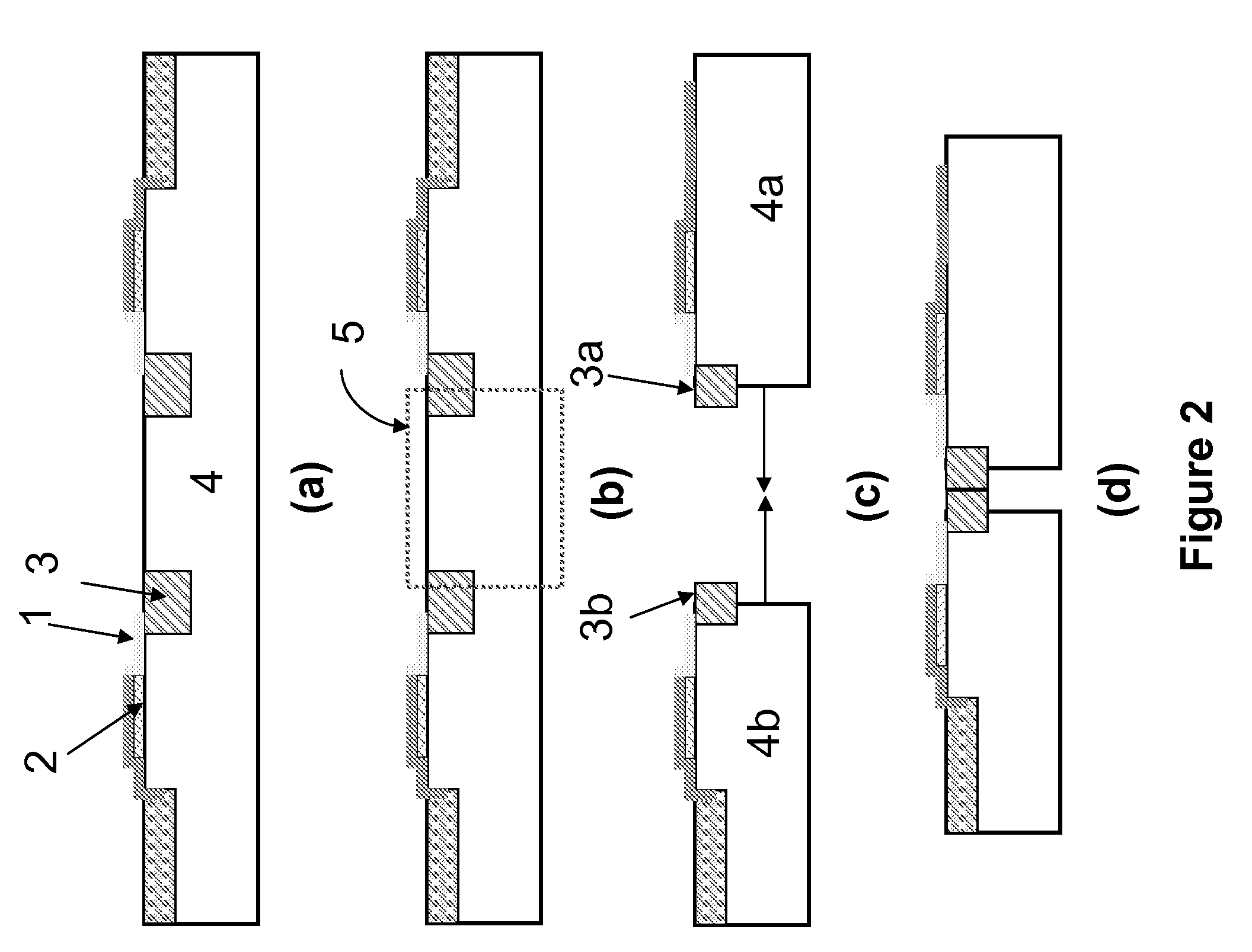
[0024]The embodiments of the present invention that are disclosed herein should be understood to be limited only by the claims that follow. Further, various terms and phrases used herein are not intended to be limiting; but rather, to provide an understandable description of the invention that could be implemented by those skilled in the art. The drawings are in simplified form, may not be to scale, and may omit certain apparatus elements and method steps, and / or may include other elements or method steps that are not shown. For clarity, directional terms, such as top, bottom, left, right, up, down, over, above, below, beneath, rear, and front may be used with respect to the accompanying drawings, and these and similar directional terms should not be construed to limit the scope of the invention in any manner. The term “coupled”, or similar terms as used herein, is defined as connected, although not necessarily directly, and not necessarily mechanically or electrically. The term “su...


PUM


Abstract

The present invention allows for direct chip-to-chip connections using the shortest possible signal path.

Description

FIELD OF THE INVENTION[0001]The present invention relates generally to interconnects and more particularly to multi-dimensional chip-to-chip interconnects.BACKGROUND OF THE INVENTION[0002]The amount of silicon “real estate” available for designers of integrated circuits (IC's) acts to limit the number of functional units (transistors, CPU's, memory, etc.) that may be fitted on any given IC. The amount of functionality can be increased by providing shorter transistor gate lengths, however, achievable device densities, as well as signal transmission speeds can be increased only so far, as the state of technology limits gate minimum length to only about 45 nm. The amount of functionality can also be increased by layering chips or dies one on top of another during front-end of the line (FEOL) processing, or by packaging and connecting multiple chips or dies via interposer chips into one discrete unit.[0003]In the layered-device approach, for example as described in U.S. Pat. No. 6,821,8...

Claims


Application Information

Patent Timeline
IPC IPC(8): H01L23/48
CPCH01L21/6835H01L24/11H01L2924/00011H01L2224/17183H01L2224/06183H01L24/81H01L24/83H01L25/0652H01L25/0655H01L25/50H01L2224/11003H01L2224/13099H01L2224/16H01L2224/8121H01L2224/81815H01L2924/01029H01L2924/01054H01L2924/01078H01L2924/01079H01L2924/01082H01L2924/14H01L2924/1532H01L2924/30105H01L2924/3025H01L2924/01005H01L2924/01006H01L2924/01024H01L2924/01033H01L2924/014H01L2224/0401H01L2224/11334H01L2924/3512H01L2924/00H01L2224/83851H01L2224/16137H01L24/97H01L2224/16238H01L2224/81005H01L2224/811H01L2224/81191H01L2224/81192H01L2224/81986H01L2224/97H01L2224/81
Inventor CORDES, STEVEN A.FARINELLI, MATTHEW J.GOMA, SHERIF A.GRUBER, PETER A.KNICKERBOCKER, JOHN U.SPEIDELL, JAMES L.
Owner GLOBALFOUNDRIES INC
Why Eureka
Try Eureka