

Semiconductor Device and Manufacturing Method Thereof
a technology of semiconductors and semiconductors, applied in semiconductor devices, electrical devices, transistors, etc., can solve problems such as the deterioration of bv (breakdown voltage) characteristics and the phenomenon of breakdown, and achieve the effect of inhibiting the ionization of impa
- Summary
- Abstract
- Description
- Claims
- Application Information
AI Technical Summary
Benefits of technology
Problems solved by technology
Method used
Image

Examples
Embodiment Construction
[0017]Hereinafter, a semiconductor device and a method for manufacturing the same according to an embodiment will be described with reference to the accompanying drawings.
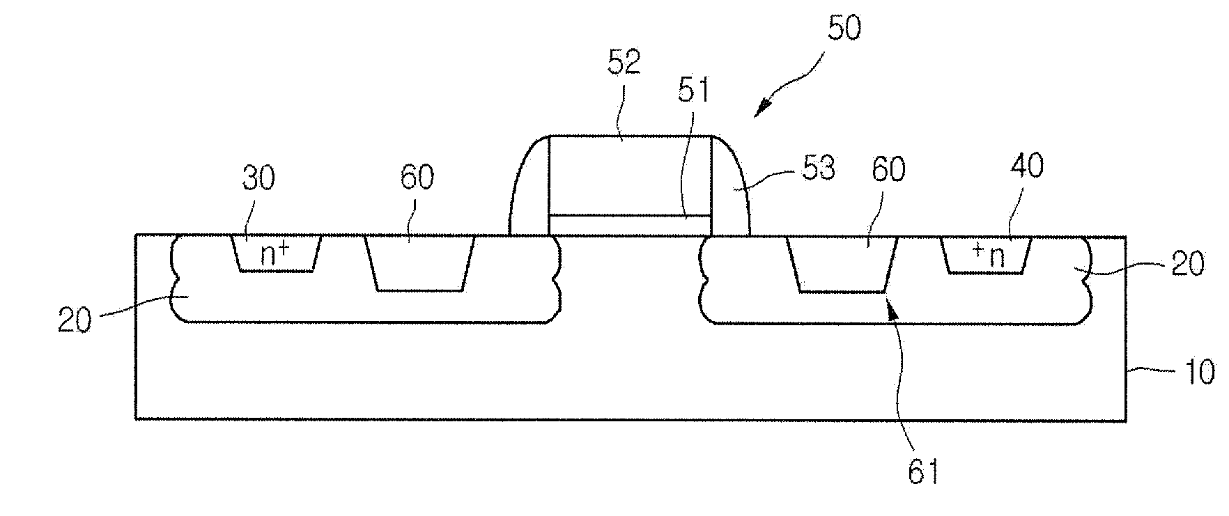
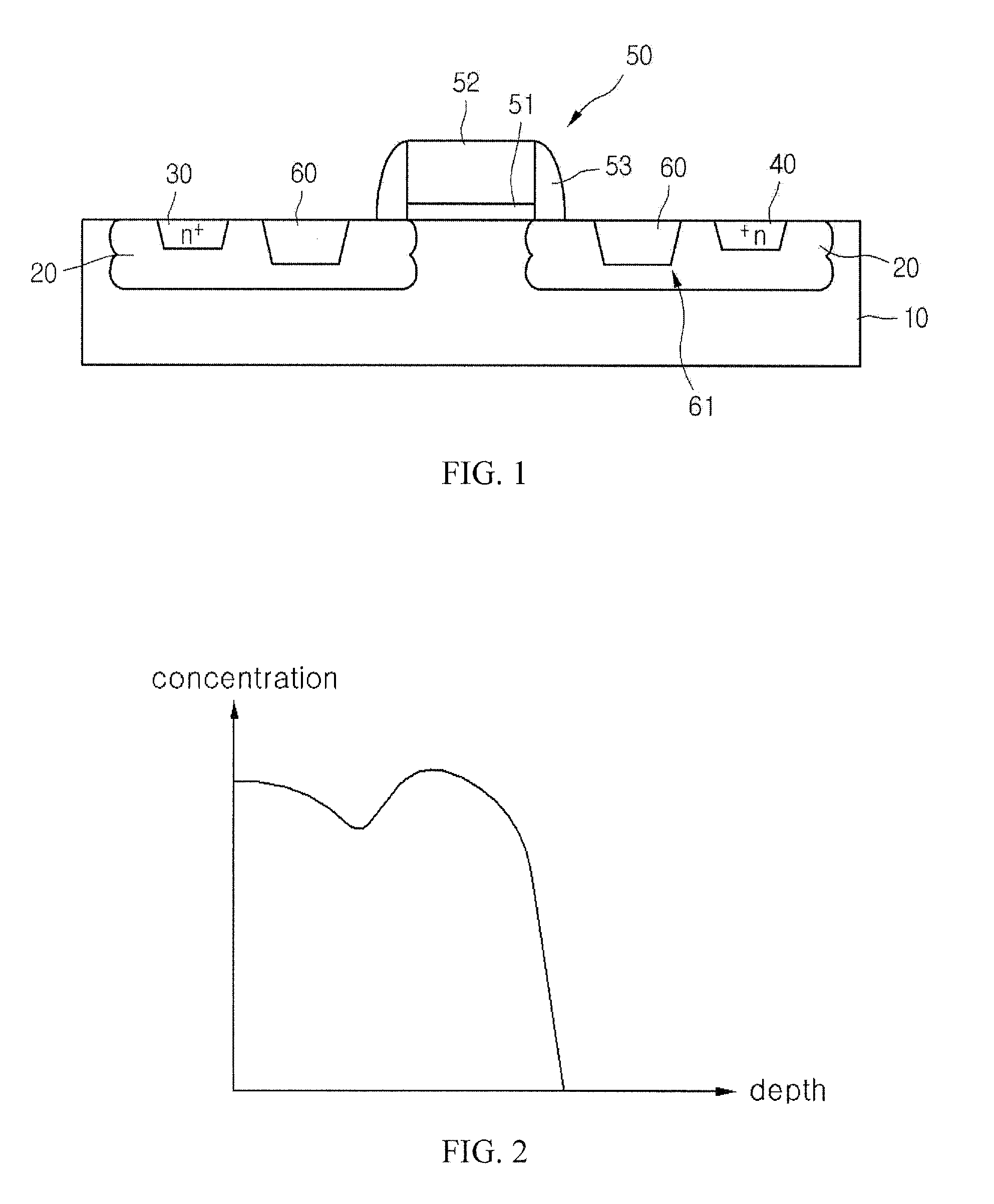
[0018]Referring to FIG. 1, a semiconductor device can include drift regions 20 formed in a semiconductor substrate 10. In one embodiment, the semiconductor substrate 10 can be P-type and the drift regions 20 can be formed of N-type impurities.
[0019]A gate electrode 50 can be provided on the substrate 10 between the drift regions 20. The gate electrode 50 can include a gate insulating layer 51, a gate poly 52, and a spacer 53. The gate poly 52 can be formed of polysilicon, metal, silicide, or a combination thereof.
[0020]A source region 30 and a drain region 40 are provided in respective portions of the drift regions 20 at each side of the gate electrode 50. The drift regions 20 can have a doping profile in which the concentration of impurities gradually increases and then decreases, and then again gradually increase...
PUM
 Abstract
Description
Claims
Application Information