

Semiconductor package and multi-chip semiconductor package using the same
a semiconductor and multi-chip technology, applied in semiconductor devices, semiconductor/solid-state device details, electrical devices, etc., can solve problems such as signal delay, noise generation, and the like, and achieve the effect of preventing signal delay and noise generation
- Summary
- Abstract
- Description
- Claims
- Application Information
AI Technical Summary
Benefits of technology
Problems solved by technology
Method used
Image

Examples
first embodiment
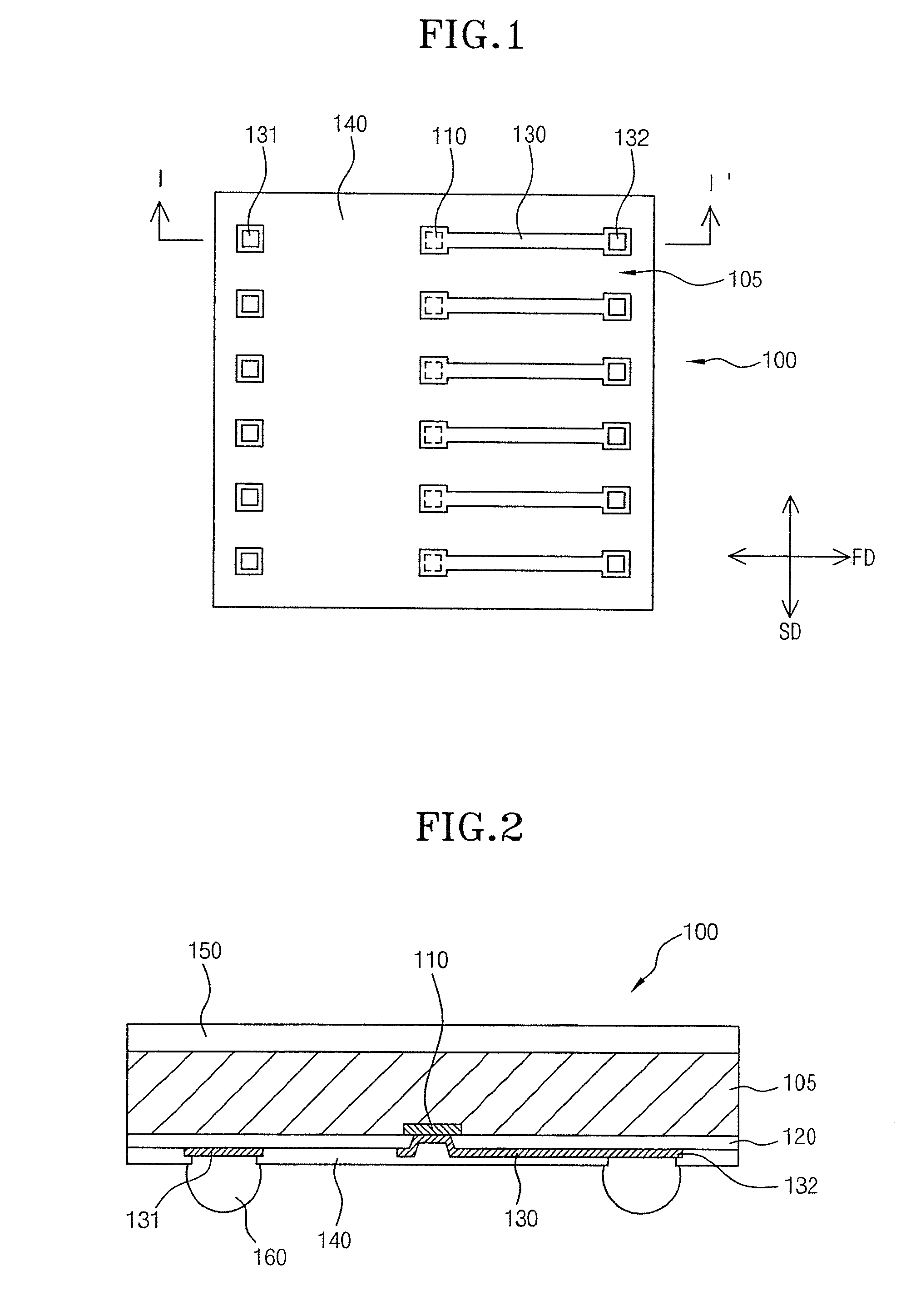
[0034]FIG. 1 is a plan view illustrating a semiconductor package in accordance with the present invention, and FIG. 2 is a cross-sectional view taken along the line I-I′ of FIG. 1, illustrating the semiconductor package with conductive balls attached thereto.
[0035]Referring to FIGS. 1 and 2, a semiconductor package 100 includes a semiconductor chip 105, redistribution patterns 130, and dummy bump pads 131.
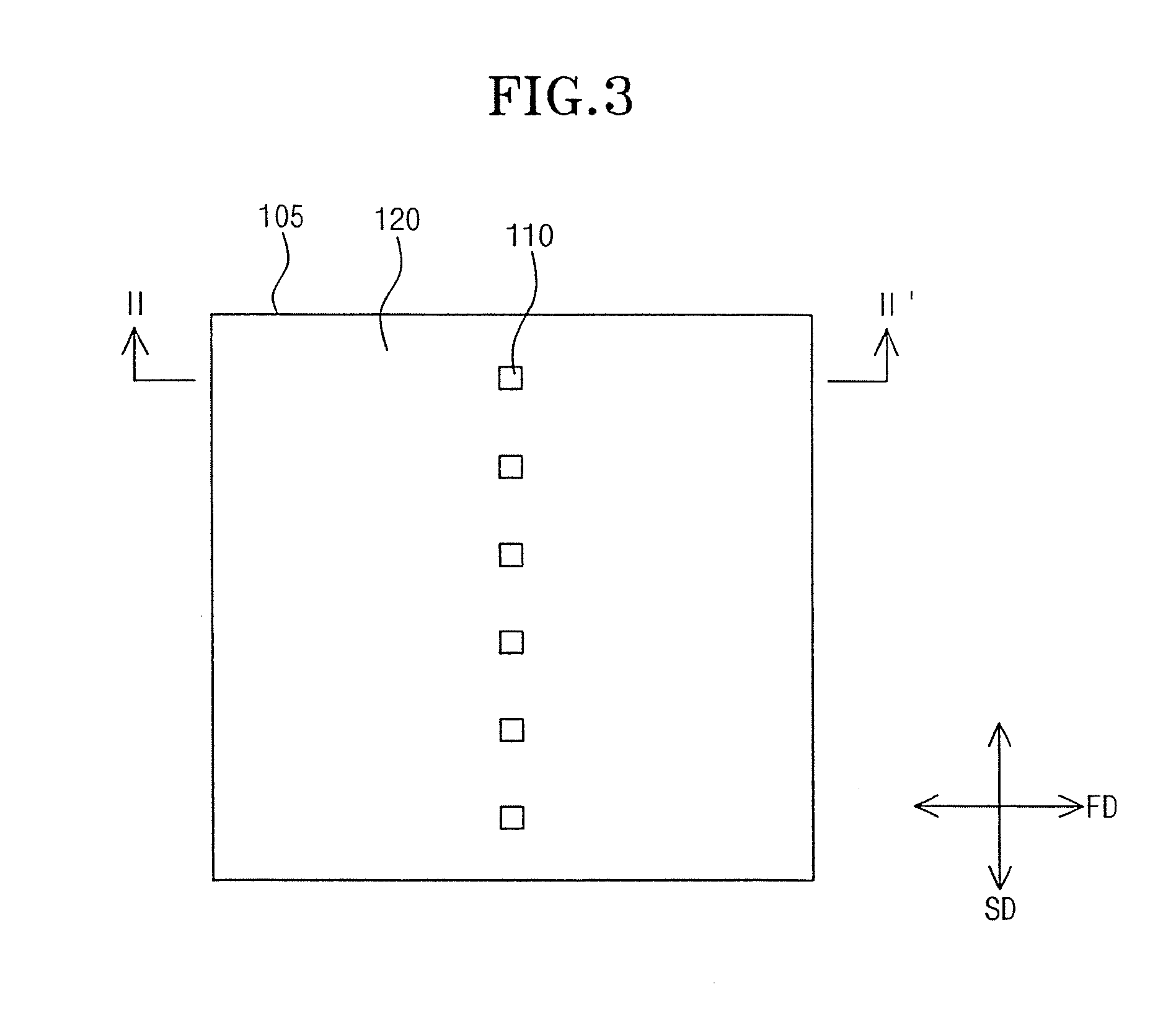
[0036]The semiconductor chip 105 has a data storage section (not shown) for storing data, a data processing section (not shown) for processing data, and one or more bonding pads 110 through which data is inputted and outputted.
[0037]The respective bonding pads 110 are located, for example, on the center portion of one surface of the semiconductor chip 105. The bonding pads 110 are located along a second direction ‘SD’ which is perpendicular to a first direction ‘FD’ in FIG. 1.
[0038]The respective bonding pads 110 are electrically connected with the data storage section and / or the d...
second embodiment
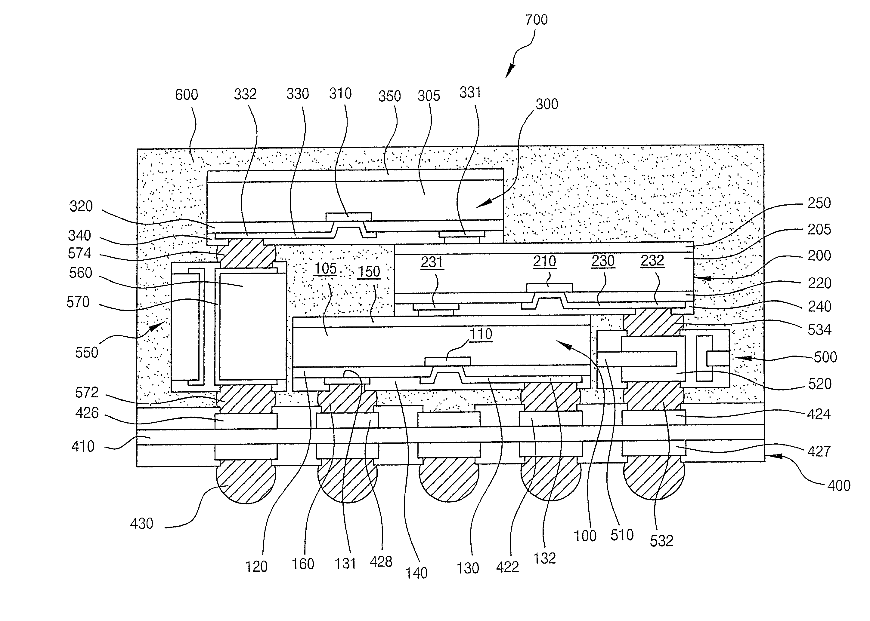
[0067]FIG. 4 is a cross-sectional view illustrating a multi-chip semiconductor package in accordance with the present invention.
[0068]Referring to FIG. 4, a multi-chip semiconductor package 700 includes semiconductor packages 100, 200 and 300, a substrate 400, a first connection substrate 500, and a second connection substrate 550. In addition, the multi-chip semiconductor package 700 may further include a molding member 600.
[0069]The substrate 400 includes an insulation substrate 410, upper connection pads 422, 424 and 426, lower connection pads 427, and conductive balls 430.
[0070]The upper connection pads 422, 424 and 426 are located on the upper surface of the insulation substrate 410. Hereafter, the respective connection pads 422, 424 and 426 will be referred to as first connection pads 422, second connection pads 424 and third connection pads 426. In addition, dummy connection pads 428 can be further formed adjacent to the first connection pads 422 among the upper connection pa...
PUM
 Abstract
Description
Claims
Application Information