Image Display Apparatus

a technology of image display and display element, which is applied in the direction of discharge tube/lamp details, nanoinformatics, discharge tube luminescnet screens, etc., can solve the problems of reducing the reliability of current feeding to the electron emission element, deficiency of current feeding capability from scan lines, etc., to improve the reliability of electron emission elements, improve current feeding capability, and improve the effect of current feeding ability

Inactive Publication Date: 2009-01-01
HITACHI LTD
View PDF3 Cites 6 Cited by
  • Summary
  • Abstract
  • Description
  • Claims
  • Application Information

AI Technical Summary

Benefits of technology

[0023]As stated above, according to this invention, a protruded portion of neighboring scan line is provided along one of longer sides of an electron emission area for functioning as the focus electrode, while providing the feeding electrode along the other longer side of the electron emission area. Use of this arrangement improves the ability to feed current from the scan line. Thus, a distribution of drive current within an electron emission-element's electrode is dispersed to thereby improve the reliability of an electron emission element. Additionally, in the case of a thin-film electron emitter being used as an electron emission element, the improvement in current feeding capability enables the top electrode to decrease in thickness, thus increasing the electron emission efficiency.

Problems solved by technology

When attempts are made to perform the focusing of an emitted electron beam by using a neighboring scan line for achievement of higher image resolution of a matrix electron emitter display apparatus, the current feeding capability from a scan line to electron emission element becomes deficient.
Another problem caused thereby is the risk of a decrease in reliability of the current feeding to the electron emission element.

Method used


Image

  • Image Display Apparatus
  • Image Display Apparatus
  • Image Display Apparatus

Examples


embodiment 1

[0061]Embodiment 1 is an example of the case where this invention is applied to a metal-insulator-metal (MIM) electron emitter display or a surface-conduction electron-emitter display (SED) or the like. The beam focusing property required in the case of a color image display apparatus will be described. In the color image display apparatus, it is an ordinary way to configure a single pixel 450 by disposing three separate sub-pixels which yield red, green, and blue light rays, respectively, as shown in FIGS. 7A-7C. In a matrix electron emitter display, a red phosphor 114A, green phosphor 114B and blue phosphor 114C are formed in respective subpixels to thereby constitute a single pixel 450.

[0062]In the matrix electron emitter display, as shown in FIGS. 7A-7C, three subpixels are disposed in a direction along a scan line (in the horizontal direction in the illustrative example) to constitute a single pixel. In particular, in the case of a line-sequential drive technique, only one (or ...

embodiment 2

[0085]In this embodiment 2, a practical arrangement of an image display apparatus using metal-insulator-metal (MIM) electron emitter also incorporating the principles of this invention will be described.

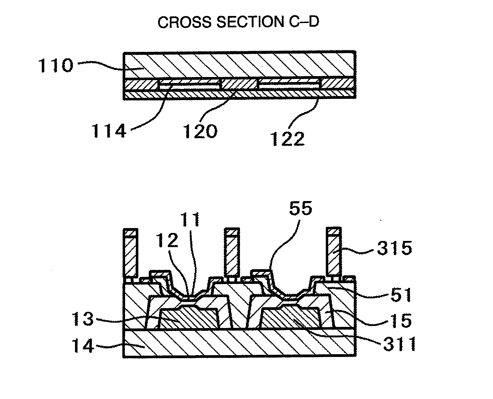
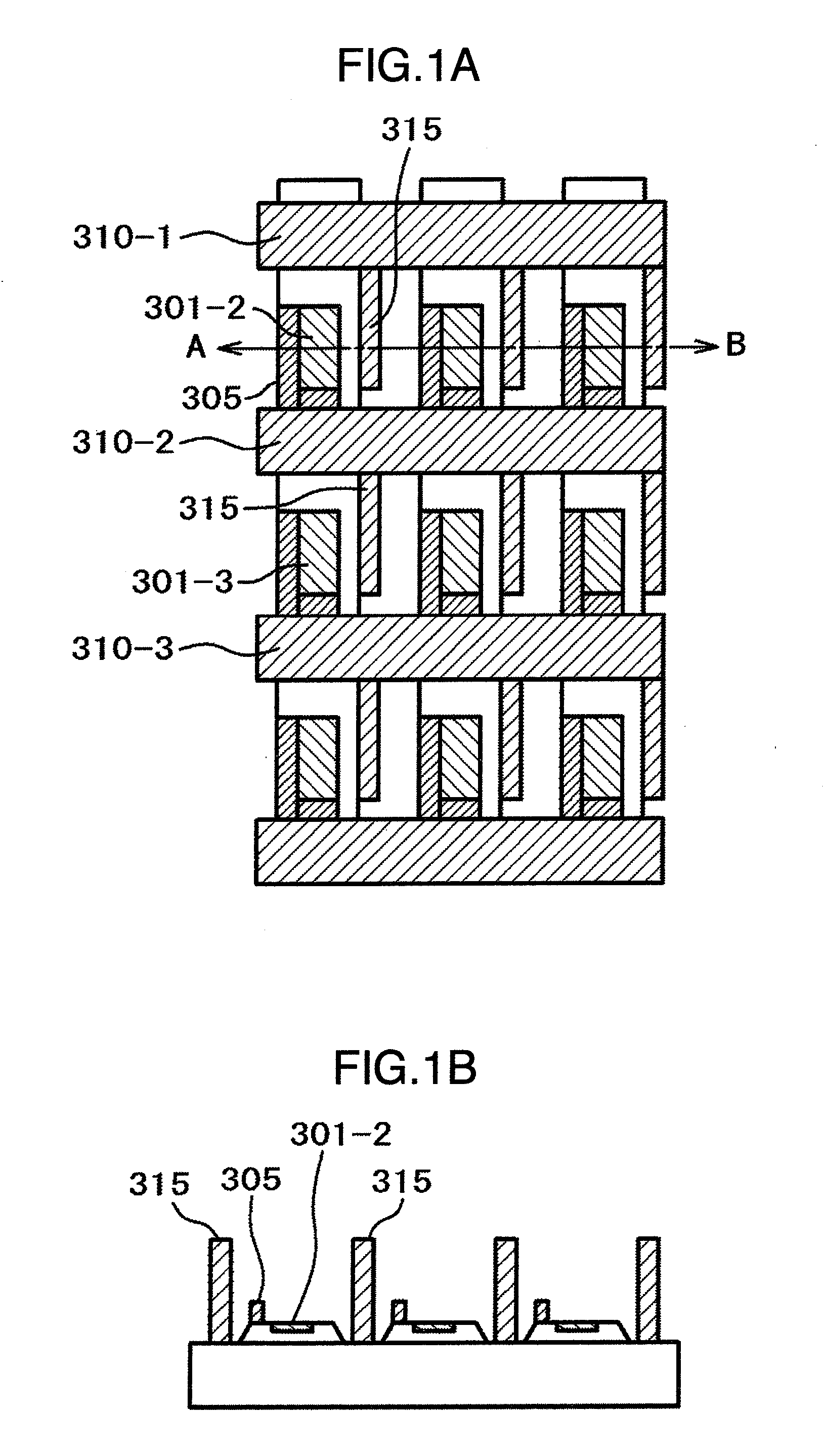
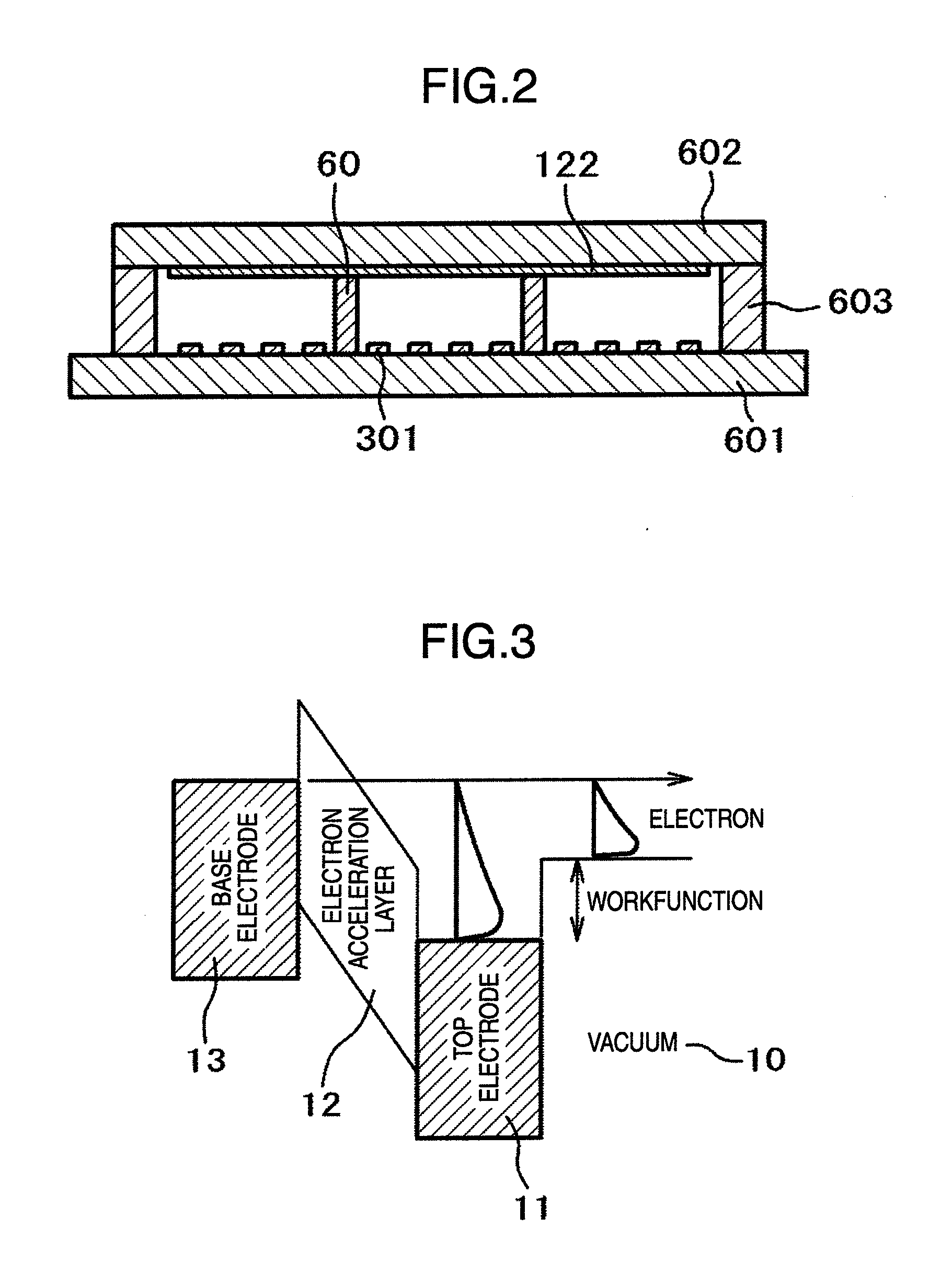
[0086]FIG. 11 is a top plan view of a display panel used in this embodiment. FIG. 12 is a cross-sectional view of the panel as taken along line A-B of FIG. 11. In FIG. 12, only scan electrodes 310 which are taken out of those constituent components of a cathode plate 601 are depicted for purposes of convenience in illustration herein. (On the contrary, in FIG. 2, only the electron emission elements 301 of the components making up the cathode plate 601 are depicted.)

[0087]An inside space that is surrounded by the cathode plate 601, a phosphor plate 602 and a frame component 603 is evacuated to a vacuum. In this vacuum region, one or more spacers 60 are disposed in order to provide increased durability against atmospheric pressures. The spacers 60 are designable and modifiable in shape...

embodiment 3

[0129]This embodiment is an example which is characterized in that the focus electrode is used to create a lateral electric field to thereby have the function of bending or curving the trajectory of an electron beam in addition to the beam focusing ability.

[0130]A top plan view of a display panel for use in this embodiment is shown in FIG. 27, and its sectional views are shown in FIGS. 28A and 28B. FIG. 27 is a plan view of part of a cathode plate 601. FIGS. 28A and 28B show sectional views of the part of cathode plate 601 corresponding to FIG. 27. FIG. 28A is a sectional view taken along line A-B of FIG. 27, and FIG. 28B is a sectional view along line C-D of FIG. 27. Note here that, in the plan view of FIG. 27, the top electrode 11 is removed for an illustrative purpose. As apparent from viewing the sectional views of FIGS. 28A and 28B, a film of top electrode 11 is formed on an overall surface.

[0131]A difference of this embodiment from the embodiment 2 shown in FIGS. 14A and 14B i...


PUM


Abstract

A protruded portion of an adjacent scan line is provided along one of longer sides of an electron emission area, for functioning as a focusing electrode. A feeding electrode is provided along the other longer side of the electron emission part. Use of this arrangement improves the ability to feed current from a scan line(s). Thus, a distribution of drive current within an element electrode is dispersed, thereby to improve the reliability of an electron emission element. Additionally, in the case of a thin-film electron source being used as this element, the improvement in current feeding ability enables a top electrode to decrease in thickness, thus increasing the electron emission efficiency.

Description

INCORPORATION BY REFERENCE[0001]The present application claims priority from Japanese application JP 2007-170012 filed on Jun. 28, 2007, the content of which is hereby incorporated by reference into this application.BACKGROUND OF THE INVENTIONField of the Invention[0002]The present invention relates to image display apparatuses of the type displaying images by using a matrix array of electron emission elements and phosphors.[0003]A matrix electron emitter display apparatus has a matrix of rows and columns of pixels at intersections of orthogonally crossing electrodes, and electron emission elements which are provided in respective pixels. An electron emitted from each electron emission element is accelerated in a vacuum while adjusting an amount of electron emission by control of either the amplitude or pulse width of a voltage being applied to each electron emission element. The accelerated electron then reaches and hits a phosphor, which thus yields light at its irradiated portion...

Claims


Application Information

Patent Timeline
Patent Type & Authority Applications(United States)
IPC IPC(8): H01J1/62
CPCB82Y10/00H01J1/312H01J1/316H01J2329/466H01J31/127H01J2329/0484H01J2329/0489H01J29/04
Inventor SUZUKI, MUTSUMISAGAWA, MASAKAZUMIKAMI, YOSHIRO
Owner HITACHI LTD
Why Eureka
Try Eureka