Light emission device and display device using the light emission device as a light source

a technology of light emission device and light emission device, which is applied in the direction of instruments, discharge tubes, luminescnet screens, etc., can solve the problems of short circuit between adjacent driving electrodes, damage to the phosphor layer, and difficulty in mounting the getter in the non-active area having a narrow width, so as to improve the emission efficiency and durability of electron emission elements, increase the adsorption efficiency of the getter, and improve the degree of vacuum of the vacuum vessel

Inactive Publication Date: 2009-01-01
SAMSUNG SDI CO LTD
View PDF14 Cites 12 Cited by
  • Summary
  • Abstract
  • Description
  • Claims
  • Application Information

AI Technical Summary

Benefits of technology

[0012]Exemplary embodiments in accordance with the present invention provide a light emission device that can enhance a degree of vacuum of a vacuum vessel by increasing adsorption efficiency of a getter, and thus improve emission efficiency and durability of electron emission elements, and a display device using the light emission device as a light source.

Problems solved by technology

However, in the former case, since there has been a tendency in recent light emission devices to reduce the width of the non-active area to minimize dead space from which visible light is not emitted, it is difficult to mount the getter in the non-active area having a narrow width.
In addition, a conductive getter material may be diffused into the active area during the getter activation process, thereby causing a short circuit between adjacent driving electrodes and damage to the phosphor layer.
In the latter case, manufacture of the vacuum vessel is complicated by adding a process for forming a hole at the rear substrate where the getter chamber is to be attached and a process for sealing the getter chamber at the exterior of the rear substrate.
Also, in both the former and latter cases, since an adsorption area of the getter is not sufficient, the getter has low adsorption efficiency.

Method used


Image

  • Light emission device and display device using the light emission device as a light source
  • Light emission device and display device using the light emission device as a light source
  • Light emission device and display device using the light emission device as a light source

Examples


Embodiment Construction

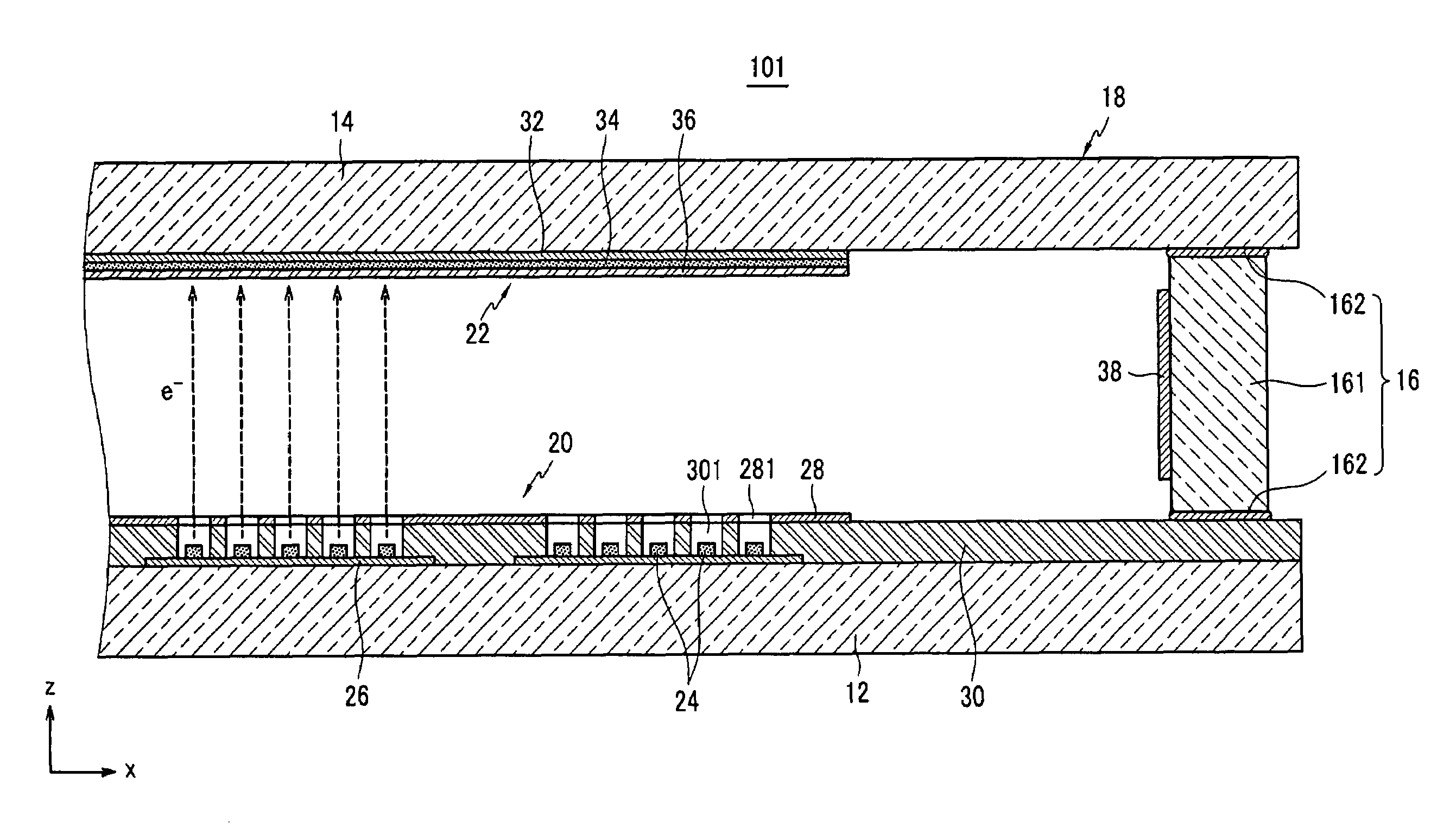
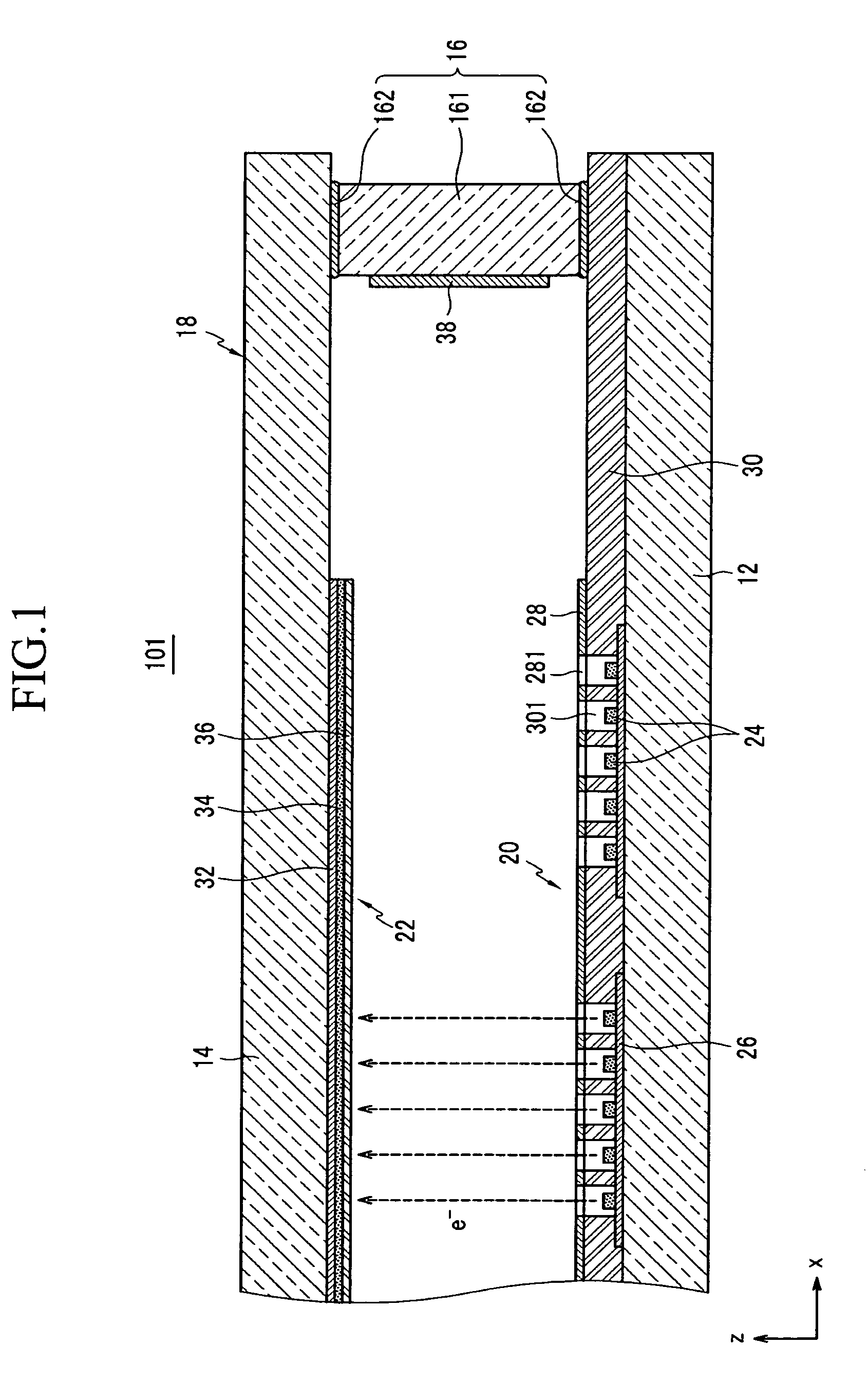
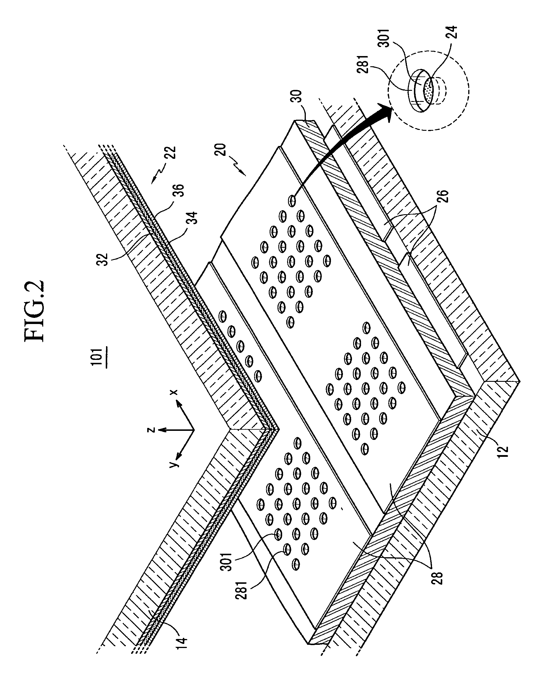
[0034]The present invention will now be described more fully with reference to the accompanying drawings, in which exemplary embodiments of the invention are shown. The invention may, however, be embodied in many different forms and should not be construed as being limited to the embodiments set forth herein; rather these embodiments are provided so that this disclosure will be thorough and complete, and will fully convey the concept of the invention to those skilled in the art.

[0035]In exemplary embodiments of the present invention, all of the light emission devices that can emit light to an external side are regarded as light emission devices. Therefore, all of display devices that can transmit information by displaying symbols, letters, numbers, and images may be regarded as the light emission devices. In addition, the light emission device may be used as a light source for emitting light to a display panel of a non-emissive type.

[0036]A light emission device of a first exemplary...


PUM


Abstract

A light emission device, which can enhance degree of vacuum in a vacuum vessel by increasing an adsorption efficiency of a getter, and a display device using the light emission device for a light source are provided. The light emission device includes a vacuum vessel having first and second substrates facing each other with a predetermined distance therebetween, and a sealing member disposed between the first and second substrates and enclosing an inner space formed between the first and the second substrates. An electron emission unit is located on one side of the first substrate and having a plurality of electron emission regions. A light emission unit is located on one side of the second substrate and having an anode electrode and a phosphor layer. A getter layer is disposed on an inner surface of the sealing member that faces an inner space of the vacuum vessel.

Description

CLAIM OF PRIORITY[0001]This application makes reference to, incorporates the same herein, and claims all benefits accruing under 35 U.S.C. §119 from an application earlier filed in the Korean. Intellectual Property Office on the 28th of June 2007 and there duly assigned Serial No. 10-2007-0064307.BACKGROUND OF THE INVENTION[0002]1. Field of the Invention[0003]The present invention relates to a light emission device having a vacuum vessel and a display device using the light emission device for a light source. The present invention further relates to a getter provided inside the vacuum vessel to adsorb gaseous molecules remaining within the vacuum vessel after an exhaust process.[0004]2. Description of Related Art[0005]There are many different types of light emission devices that radiate visible light. One type of light emission device includes a structure in which a light emission unit having an anode electrode and a phosphor layer is disposed on a front substrate, and an electron e...

Claims


Application Information

Patent Timeline
Patent Type & Authority Applications(United States)
IPC IPC(8): H01J1/62H01J29/94H01J31/12
CPCG02F1/133602G02F2001/133612G09G3/3413H01J63/06G09G2300/0426H01J61/26H01J61/305G09G3/3426G02F1/133612
Inventor SONG, GI-YOUNG
Owner SAMSUNG SDI CO LTD
Why Eureka
Try Eureka