Probe resistance measurement method and semiconductor device with pads for probe resistance measurement

a technology of resistance measurement and probe, which is applied in the direction of resistance/reactance/impedence, semiconductor/solid-state device details, instruments, etc., can solve the problems of inability to meet the measurement requisition, the voltage drop due to the contact resistance cannot be ignored, and the current reduces at a considerable ra

Inactive Publication Date: 2009-01-08
RENESAS ELECTRONICS CORP
View PDF3 Cites 25 Cited by
  • Summary
  • Abstract
  • Description
  • Claims
  • Application Information

AI Technical Summary

Benefits of technology

[0013]In a first aspect of the present invention, a probe resistance measuring method includes measuring first resistances at three or more nodes by making contact at least a part of a plurality of probes of a probe unit with three or more pads for resistance measurement based on a first correspondence relation; storing the measured first resistances as a first measurement result; and calculating contact resistances of the plurality of probes of the probe unit based on the first measurement result.
[0014]In a second aspect of the present invention, a semiconductor device with pads for probe resistance measurement, includes three or more pads electrically isolated from a semiconductor circuit formed on a semiconductor substrate; and wiring lines provided to connect between the pads in series and having a same resistance.

Problems solved by technology

Accordingly, it is impossible to meet the measurement requisition only by an open / short check and a rough check of resistance between pads.
Therefore, when a contact resistance of about 10Ω is attached to the probe, a voltage drop due to the contact resistance cannot be ignored, because the current reduces at a considerable rate.
Also, in a technique described in this first related art, it is not possible to measure the contact resistance of each probe precisely.
However, in this method, the contact resistances of all the probes are not measured and cannot be determined.
In this technique, a resistance between two pads, a contact state and needle pressure can be detected, but the contact resistance of each probe cannot be determined precisely.
In this technique, a contact state of a probe group can be checked but the contact resistance of each probe cannot be determined precisely.

Method used


Image

  • Probe resistance measurement method and semiconductor device with pads for probe resistance measurement
  • Probe resistance measurement method and semiconductor device with pads for probe resistance measurement
  • Probe resistance measurement method and semiconductor device with pads for probe resistance measurement

Examples


first embodiment

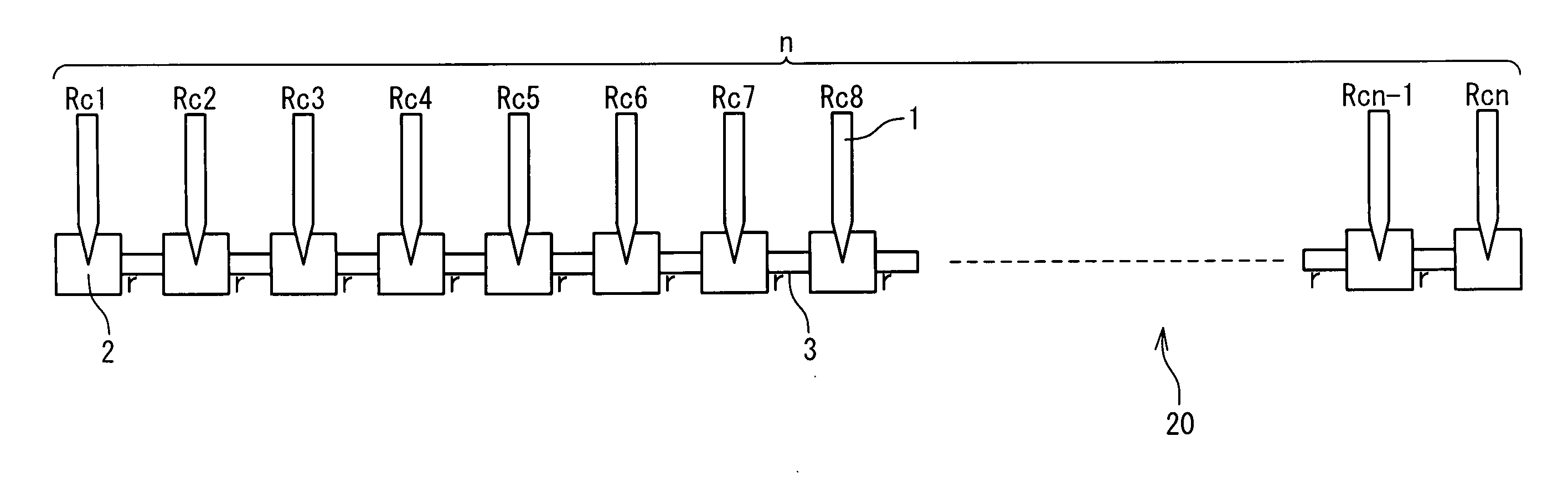
[0043]FIG. 7A is a diagram showing a probe unit having n (n≧3) probes. As shown in FIG. 7A, m (m≧3, and it is not necessary to be n=m) pads connected in series are provided for the probe unit having the n probes. A test element group (hereinafter, to be referred to as a TEG) 20 for contact resistance measurement is arranged in which resistances between the pads 2 (resistances of wiring lines 3) are equal to each other. The contact resistance of each of the n probes 1 is measured by the probe unit and the pads 2. The measured contact resistance contains the resistance of a resistor from the tip of probe 1 to a wiring line of a device through the probe unit.

(a) Case of n≧4 and n≦m

[0044]Numbers 1, 2, 3 . . . are allocated to the pads 2 in order from the pad 2 arranged at the end of the TEG 20 for contact resistance measurement. First, the four pads 2 connected in series and having the numbers 1 to 4 are selected. The measured resistances between No. 1 and No. 2, between No. 2 and No. 3...

second embodiment

[0059]As shown in FIGS. 8A and 8B, it is possible to measure the contact resistances of the probes while rotating a wafer by 180 degrees. As shown in FIG. 8A, the TEG composed of n pads (n is an even number) is used in this embodiment. The TEG is composed of a TEG 20 for contact resistance measurement of the n / 2 pads 2 from the one end and a TEG 21 for device characteristic evaluation of the n / 2 pads from the other end. The structure of the TEG 20 for contact resistance measurement is same as that of the TEG shown in FIG. 7A.

[0060]First, n / 2 of the n probes 1 are made contact with the TEG 20 for contact resistance measurement, and the contact resistances are measured by the method of described in the first embodiment. After that, by using the characteristic of an auto-prober, the wafer is rotated by 180 degrees and the remaining n / 2 probes 1 are made contact with the TEG 20 for contact resistance measurement to measure the contact resistances. The contact resistances of all of the n...

third embodiment

[0062]As shown in FIG. 9, it is not necessary to arrange the pads 2 on a straight line and the pads 2 may be arranged on a curved line. By laying out the pads such that the resistances between adjacent pads 2 are equal to each other, the contact resistances of probes 1 can be measured, as in FIG. 7A.


PUM


Abstract

A probe resistance measuring method includes measuring first resistances at three or more nodes by making contact at least a part of a plurality of probes of a probe unit with three or more pads for resistance measurement based on a first correspondence relation. The measured resistances are stored as a first measurement result and contact resistances of the plurality of probes of the probe unit are calculated based on the first measurement result.

Description

BACKGROUND OF THE INVENTION[0001]1. Field of the Invention[0002]The present invention is relates to a technique for evaluating electric characteristics of a device. This US patent application is based on Japanese Patent application Nos. 2007-099090 and 2008-065625. The disclosure thereof is incorporated herein by reference.[0003]2. Description of Related Art[0004]In order to evaluate the electric characteristics of a device, a method of making probes contact pads to measure a resistance between wiring lines is carried out. At this time, a contact resistance of the probe influences the measurement resistance. With influence of the probe contact resistance on an automatic measuring apparatus, even if an unnecessary resistance is added to the probe in the form of contamination to shift the electric characteristics a little bit, the measurement value falls within a manufacturing deviation and any problem is not caused.[0005]However, recently, it is required to reduce the deviation with ...

Claims


Application Information

Patent Timeline
Patent Type & Authority Applications(United States)
IPC IPC(8): G01R27/02H01L23/58
CPCG01R27/205G01R31/2853G01R31/2884G01R35/00H01L2924/0002H01L2924/00
Inventor MICHIMATA, SHIGETOMIYANAGISAWA, MASAYUKIKUROYANAGI, KAZUMASA
Owner RENESAS ELECTRONICS CORP
Why Eureka
Try Eureka