
Ceramic member, member for semiconductor manufacturing apparatus, and method for manufacturing ceramic member

Active Publication Date: 2014-10-02
NGK INSULATORS LTD
View PDF7 Cites 7 Cited by
  • Summary
  • Abstract
  • Description
  • Claims
  • Application Information

AI Technical Summary

Benefits of technology

The present invention provides a ceramic member with a more stable electrode that can withstand exposure to reactive plasma used in semiconductor manufacturing. The ceramic base includes components that provide higher moisture resistance and water resistance than magnesium oxide. The ceramic member is chemically unreactive with the electrodes and has a controllable thermal expansion coefficient, which ensures electrical conductivity and reduces cracking in the surrounding area. The ceramic member can effectively suppress cracking caused by high temperatures and exposure to reactive plasma. The electrode can be made of nitrides, carbides, carbonitrides, or metals.

Problems solved by technology

These materials are gradually corroded in long-term use and generate dust.
Thus, the surface of magnesium oxide gradually deteriorates (a moisture resistance problem).
When magnesium oxide is used in a member for a semiconductor manufacturing apparatus, therefore, semiconductor devices may be contaminated by decomposition gases of the hydroxide and carbonate or by magnesium oxide particles or dust formed by the decomposition of the hydroxide and carbonate.
This retards the practical application of magnesium oxide.

Method used


Image

  • Ceramic member,  member for semiconductor manufacturing apparatus, and method for manufacturing ceramic member
  • Ceramic member,  member for semiconductor manufacturing apparatus, and method for manufacturing ceramic member
  • Ceramic member,  member for semiconductor manufacturing apparatus, and method for manufacturing ceramic member

Examples


examples

[0042]Preferred applications of the present invention will be described below. Experimental Examples 1 to 27 describe the results of the more specific study on ceramic bases. In Experimental Examples 1 to 16 and 23 to 27, at least 99.9 mass % pure commercial products having an average particle size of 1 μm or less were used as a MgO raw material and an Al2O3 raw material, and a 99 mass % pure commercial product having an average particle size of 1 μm or less was used as an AlN raw material. In Experimental Examples 17 to 22, a 99.4 mass % pure commercial product having an average particle size of 3 μm was used as a MgO raw material, a 99.9 mass % pure commercial product having an average particle size of 0.5 μm was used as an Al2O3 raw material, and the commercial product having an average particle size of 1 μm or less used in Experimental Examples 1 to 16 and 23 to 27 was used as an AlN raw material. Experimental Examples 1 to 4, 7 to 17, 21, and 23 to 27 corresponded to examples o...

experimental examples 1 to 16 and 25

Compounding

[0043]The MgO raw material, the Al2O3 raw material, and the AlN raw material were weighed at the mass percentages listed in Table 1 and were wet-blended in an isopropyl alcohol solvent in a nylon pot using alumina rounded stones having a diameter of 5 mm for four hours. After blending, the resulting slurry was removed and was dried in a nitrogen stream at 110° C. The dried product was passed through a 30-mesh sieve to yield a mixed powder. The mixed powder had a Mg / Al molar ratio of 2.9.

Molding

[0044]The mixed powder was uniaxially pressed at a pressure of 200 kgf / cm2 to form a disc-shaped compact having a diameter of 50 mm and a thickness of approximately 20 mm. The disc-shaped compact was placed in a graphite mold for firing.

Firing

[0045]The disc-shaped compact was subjected to hot-press firing to manufacture a ceramic base. The hot-press firing was performed at a pressing pressure of 200 kgf / cm2 at a firing temperature (maximum temperature) listed in Table 1 in an Ar atm...

experimental example 22

[0047]A mixed powder was prepared in a compounding process in the same manner as in Experimental Example 1 except that the MgO raw material and the Al2O3 raw material were weighed at the mass percentages listed in Table 1. The mixed powder was uniaxially pressed at a pressure of 100 kgf / cm2 to form a cylindrical compact having a diameter of 20 mm and a thickness of approximately 15 mm. The compact was subjected to a CIP forming process at 3000 kgf / cm2. A graphite crucible having a lid was charged with the mixed raw materials. The compact was then buried in the mixed raw materials. The cylindrical compact was fired at normal pressure in a firing process to manufacture a ceramic base. In the firing process, the cylindrical compact was fired at the firing temperature (maximum temperature) listed in Table 1 in an Ar atmosphere to the completion of firing. The holding time at the firing temperature was four hours.

[0048][Evaluation]

[0049]The materials prepared in Experimental Examples 1 t...


PUM

PropertyMeasurementUnit
Percent by massaaaaaaaaaa

Abstract

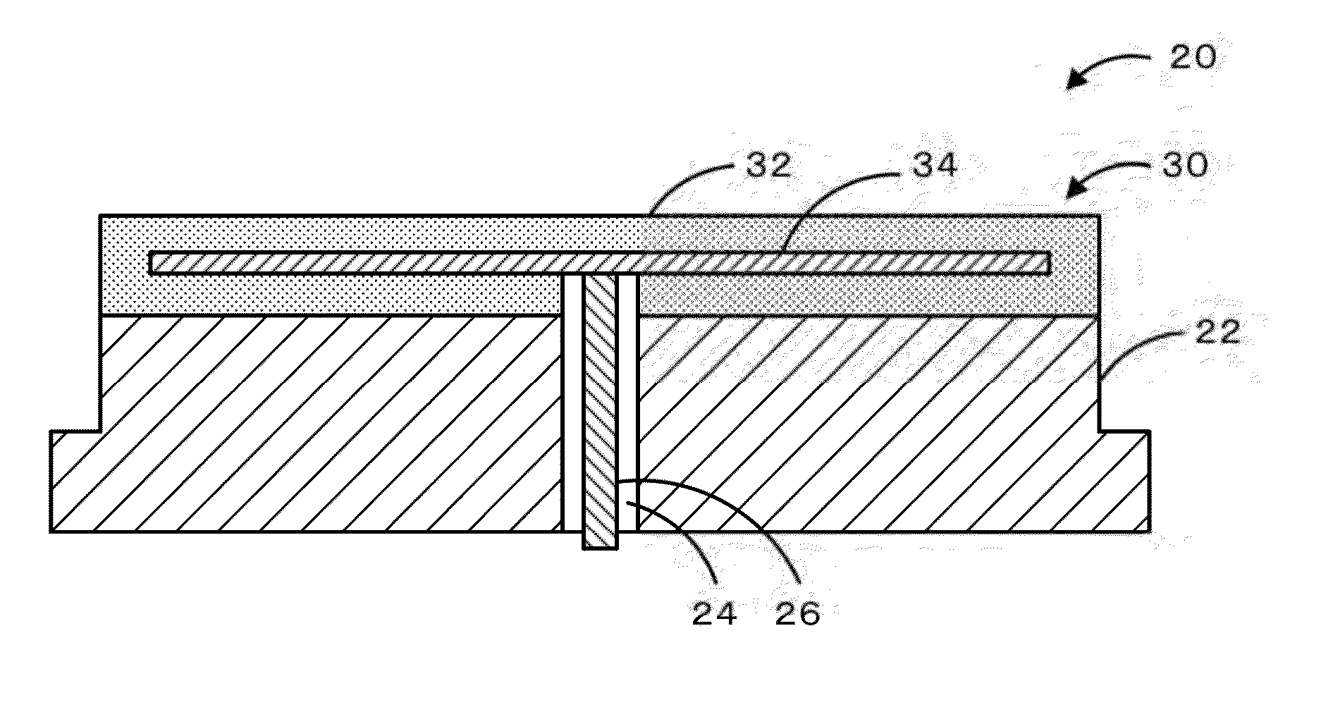
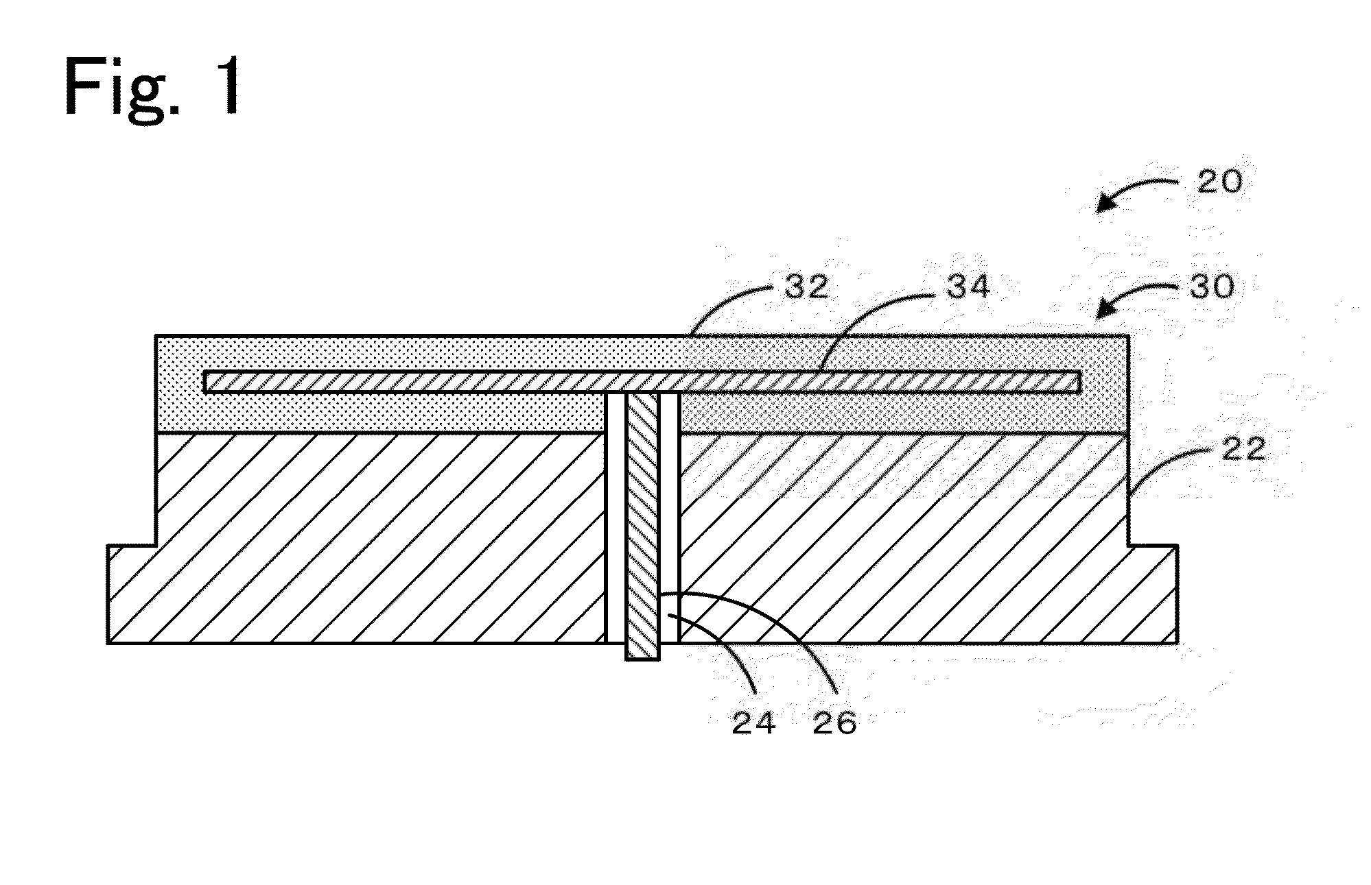
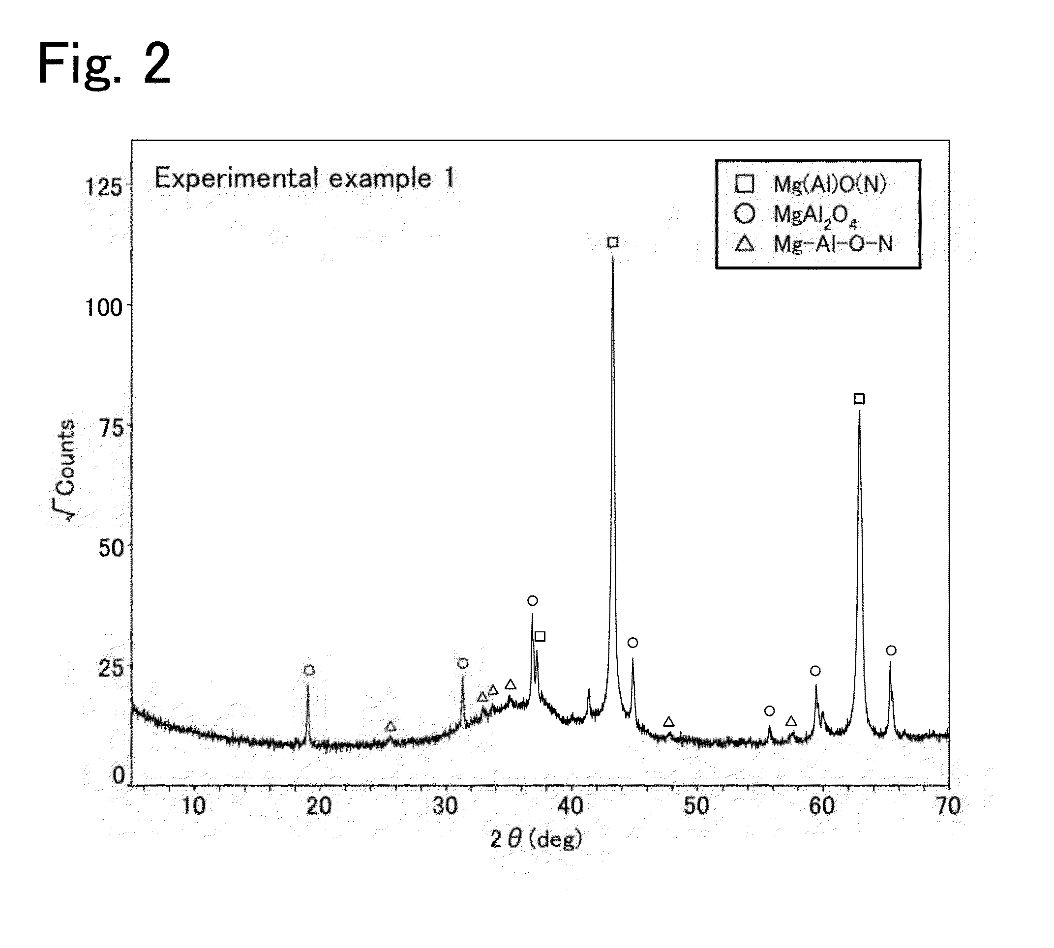
A ceramic member 30 according to the present invention includes a ceramic base 32, which contains a solid solution Mg(Al)O(N) in which Al and N components are dissolved in magnesium oxide as the main phase, and an electrode 34 disposed on a portion of the ceramic base 32 and containing at least one of nitrides, carbides, carbonitrides, and metals as an electrode component. The ceramic base 32 may have an XRD peak of a (111), (200), or (220) plane of Mg(Al)O(N) measured using a CiKα ray at 2θ=36.9 to 39, 42.9 to 44.8, or 62.3 to 65.2 degrees, respectively, between a magnesium oxide cubic crystal peak and an aluminum nitride cubic crystal peak.

Description

FIELD OF THE INVENTION[0001]The present invention relates to a ceramic member, a member for a semiconductor manufacturing apparatus, and a method for manufacturing the ceramic member.BACKGROUND OF THE INVENTION[0002]Reactive plasma of a halogen, such as F or Cl, for etching or cleaning is used in a semiconductor manufacturing apparatus for use in a dry process or plasma coating in semiconductor manufacturing. Thus, members for use in such a semiconductor manufacturing apparatus require high corrosion resistance and generally include members composed of corrosion-resistant metals, such as Al subjected to alumite treatment and Hastelloy, and ceramics. In particular, electrostatic chuck members and heater members for supporting and fixing a Si wafer require high corrosion resistance and low dusting and are therefore made of corrosion-resistant ceramics, such as aluminum nitride, alumina, and sapphire. These materials are gradually corroded in long-term use and generate dust. Thus, ther...

Claims


Application Information

Patent Timeline
IPC IPC(8): H01L21/683
CPCH01L21/6831C04B35/053C04B35/58C04B2235/3217C04B2235/3222C04B2235/3865C04B2235/6586C04B2235/76C04B2235/77C04B2235/80C04B2235/9607H01L21/6833
Inventor WATANABE, MORIMICHIJINDO, ASUMIKATSUDA, YUJISATO, YOSUKEISODA, YOSHINORIWATANABE, ATSUSHI
Owner NGK INSULATORS LTD
Learn More