Ceramic substrate and manufacturing method therefor

a technology of ceramic substrate and manufacturing method, which is applied in the direction of insulating substrate metal adhesion improvement, transfer patterning, circuit masks, etc., can solve the problems of ceramic base delamination, increase in product cost, and metal layer cracks may occur in the metal layer, so as to improve the electrical characteristics such as electric conductivity, thermal resistance, and increase the area

Active Publication Date: 2020-10-01
AMOSENSE
View PDF0 Cites 10 Cited by
  • Summary
  • Abstract
  • Description
  • Claims
  • Application Information

AI Technical Summary

Benefits of technology

[0036]According to the present invention, the ceramic substrate and the manufacturing method thereof according to the embodiment of the present invention are advantageous over a dimple-type ceramic AMB substrate according to the related art in that the metal layer is increased in area, leading to improvement in electric characteristics such as electric conductivity, thermal resistance, and the like while realizing the same level of crack resistance and delamination resistance as the dimple-type ceramic AMB substrate according to the related art.
[0037]Furthermore, the ceramic substrate and the manufacturing method thereof according to the embodiment of the present invention are advantageous over the dimple-type ceramic AMB substrate according to the related art in that the ceramic substrate has a relatively large area Because of this, when electrical characteristics thereof are the same, it is possible to realize relatively high crack and delamination resistance.
[0038]Furthermore, the ceramic substrate and the manufacturing method thereof according to the embodiment of the present invention are advantageous over the dimple-type ceramic AMB substrate according to the related art in that the ceramic substrate has a relatively large area, making it possible to strongly maintain the strength and bonding strength and find application in forming of a micro-scale pattern.
[0039]Furthermore, the ceramic substrate and the manufacturing method thereof according to the embodiment of the present invention are advantageous over the dimple-type ceramic AMB substrate according to the related art in terms of securing reliability while providing a prolonged lifespan.
[0040]Furthermore, in the ceramic substrate and the manufacturing method therefor according to the embodiment of the present invention, controlling an etching pattern of the mask (that is, a dry film) is possible upon forming the inclined protrusion, thus making it unnecessary to perform additional etching two or three times and thus leading to a reduction in post-processing cost.
[0041]Furthermore, in the ceramic substrate and the manufacturing method therefor according to the embodiment of the present invention, forming the inclined protrusion in the metal makes it possible to disperse energy on the boundary surface of the metal layer, thus improving long-term reliability of an AMB insulated gate bipolar mode transistor (IGBT) substrate.

Problems solved by technology

Because of this, when a rapid temperature change occurs, cracks may occur in the metal layer or delamination of the metal layer from the ceramic base may occur.
However, such Si3N4 and SiC have high strength but are costly, leading to an increase in product cost and thus a decrease in product competitiveness.
However, the dimple-type ceramic AMB substrate is problematic in that formation of the multiple dimples may lead to a decreased area of the metal layer, thus leading to a degradation in electrical characteristics such as electric conductivity, thermal resistance, and the like.
In other words, the electrical characteristics of the ceramic AMB substrate are proportional to the area of the metal layer, and thus in the dimple-type ceramic AMB substrate, the metal layer may decrease in area due to the multiple dimples formed along the boundary surface of the metal layer, leading to deteriorated electrical characteristics.
Furthermore, the dimple-type ceramic AMB substrate is also problematic in that when the dimples are formed only in a part of the metal layer in order to prevent the deterioration in electrical characteristics, a part of the metal layer having no dimples may undergo cracking or delamination from the ceramic base.
Furthermore, the dimple-type ceramic AMB substrate is still problematic in that the dimples has a high area ratio, leading to an increase in resistance and a decrease in strength and in bonding strength between the ceramic base and the metal layer, thereby failing to satisfy the electrical characteristics required according to application purpose.
Furthermore, the dimple-type ceramic AMB substrate does not find application in forming of a micro-scale pattern due to the high area ratio of the dimples.

Method used


Image

  • Ceramic substrate and manufacturing method therefor
  • Ceramic substrate and manufacturing method therefor
  • Ceramic substrate and manufacturing method therefor

Examples


Embodiment Construction

[0051]Hereinbelow, exemplary embodiments of the present invention will be described in detail with reference to the accompanying drawings such that the invention can be easily embodied by one of ordinary skill in the art to which this invention belongs. Reference now should be made to the drawings, in which the same reference numerals are used throughout the different drawings to designate the same or similar components. In the following description, it is to be noted that, when the functions of conventional elements and the detailed description of elements related with the present invention may make the gist of the present invention unclear, a detailed description of those elements will be omitted.

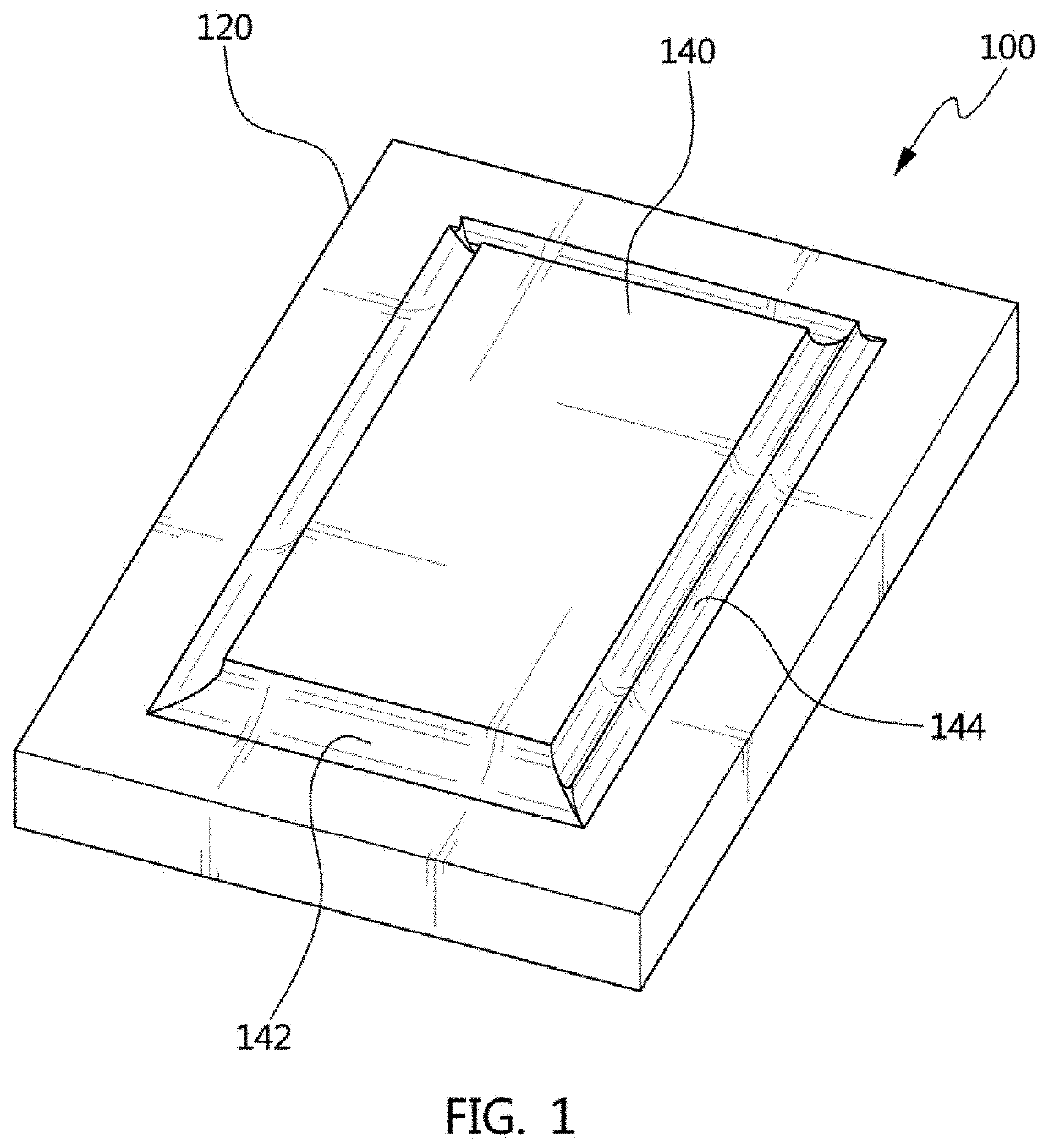
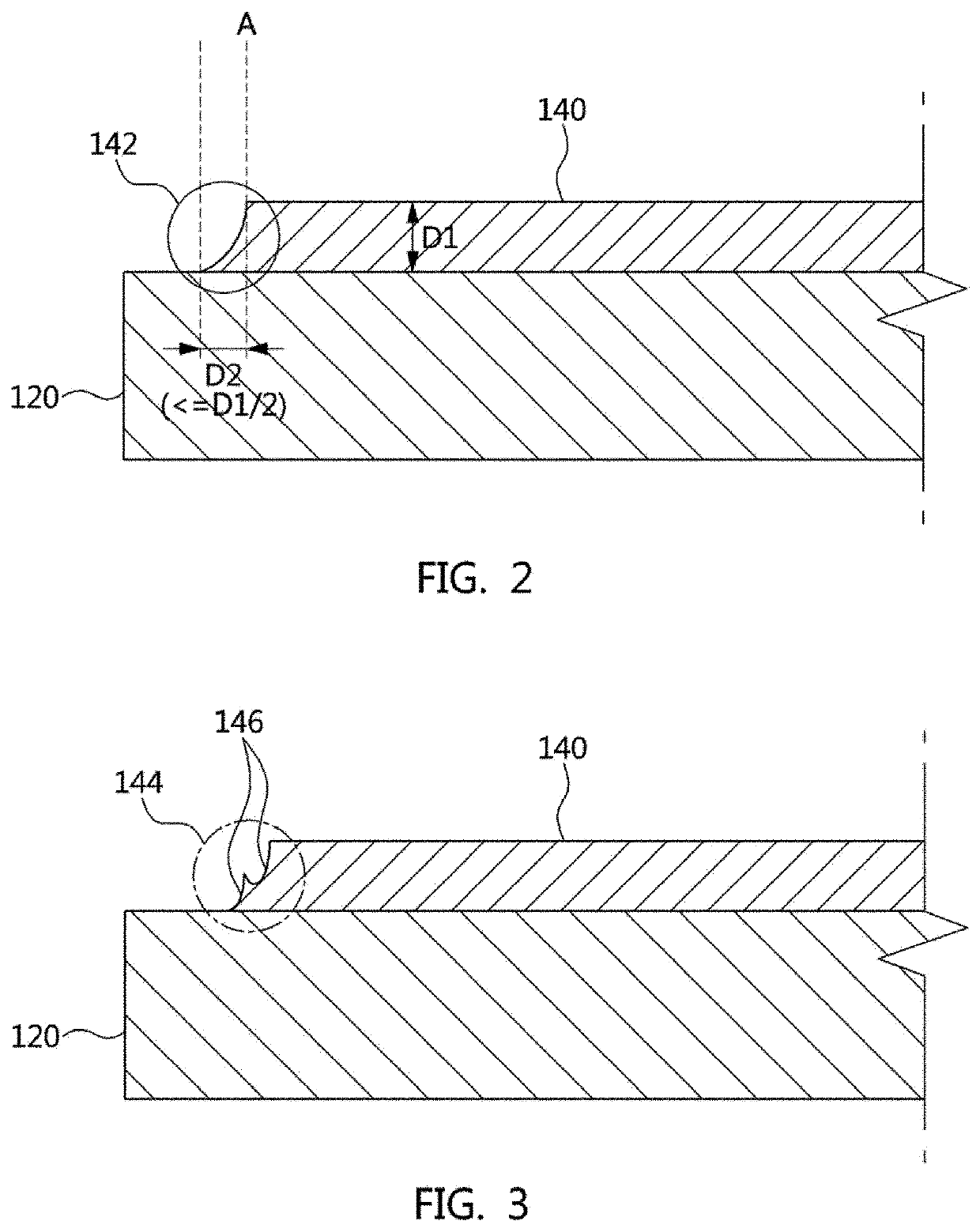
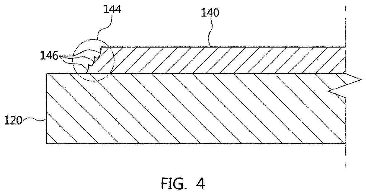
[0052]Referring to FIG. 1, a ceramic substrate 100 according to an embodiment of the present invention includes a ceramic base 120 and a metal layer 140.

[0053]The ceramic base 120 is made of a ceramic material such as zirconia toughened alumina (ZTA), aluminum nitride (AlN), aluminum oxid...


PUM

PropertyMeasurementUnit
inclination angleaaaaaaaaaa
temperatureaaaaaaaaaa

Abstract

A ceramic substrate is provided in which an inclined protrusion is formed on boundary surface of a metal layer bonded to a ceramic base so as to increase bonding strength; and a manufacturing method therefor. The inclined protrusion may include: a tapered protrusion and a multi-stepped protrusion formed on the boundary surface of the metal layer according to an interval between the metal layer bonded to the ceramic base and a neighboring metal layer, wherein a multi-stepped protrusion having an inclination angle within a predetermined angle range with respect to the ceramic base may be formed on the boundary surface of the metal layer where stress is concentrated, such as the short edge, apex, corner, and the like, and a tapered protrusion may be formed on a remaining portion of the boundary surface of the metal layer.

Description

TECHNICAL FIELD[0001]The present invention relates to a ceramic substrate and a manufacturing method therefor. More particularly, the present invention relates to a ceramic substrate and a manufacturing method therefor, in which a bonding state between a ceramic base and a metal film is firmly maintained even under a rapid temperature change.CROSS REFERENCE TO RELATED APPLICATION[0002]The present application claims priority to Korean Patent Application No. 10-2016-0077297, filed Jun. 21, 2016, Korean Patent Application No. 10-2016-0111098, filed Aug. 30, 2016, and Korean Patent Application No. 10-2016-0128623, filed Oct. 15, 2016, the entire contents of which is incorporated herein for all purposes by this reference.BACKGROUND ART[0003]As well known in the art, a ceramic substrate is formed by integrally bonding a metal foil such as a copper foil to a ceramic base. The ceramic substrate is manufactured through manufacturing processes such as active metal brazing (AMB) and direct bon...

Claims


Application Information

Patent Timeline
Patent Type & Authority Applications(United States)
IPC IPC(8): H05K1/02H05K1/03H05K3/02H05K3/38H05K3/06H01L23/498
CPCH05K2201/09827H05K3/381H05K3/067H05K3/061H05K1/0306H05K1/0296H01L23/49838H05K3/022H05K1/0271H05K3/0079H05K3/388H05K2203/0346H05K2203/0528H05K2203/0789
Inventor LEE, JI-HYUNGPARK, IK-SEONGCHO, HYEON-CHOON
Owner AMOSENSE
Why Eureka
Try Eureka