

Ultra slim semiconductor package and method of fabricating the same
a semiconductor and ultra-slim technology, applied in semiconductor devices, semiconductor/solid-state device details, electrical devices, etc., can solve the problems of reducing the size and thickness of the whole package, unable to meet the requirements of various application devices, and the substrate becomes an obstacle in the development of communication devices or electronic devices
- Summary
- Abstract
- Description
- Claims
- Application Information
AI Technical Summary
Problems solved by technology
Method used
Image

Examples
first embodiment
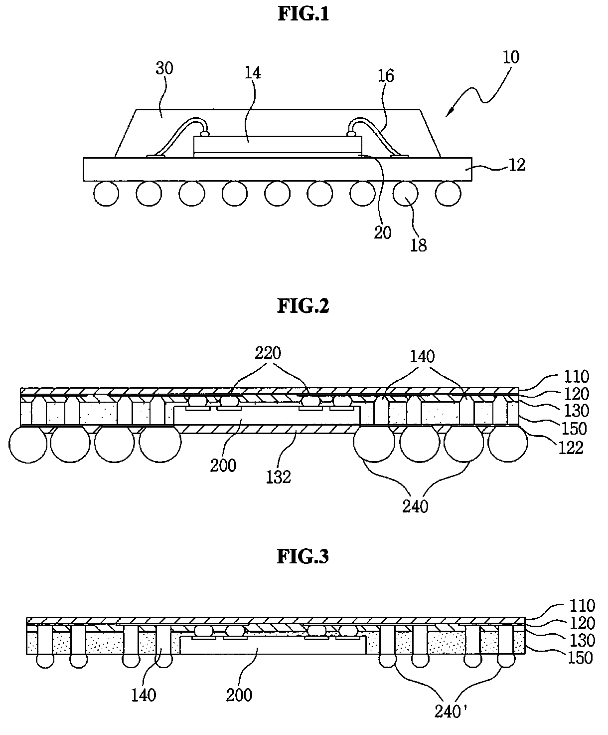
[0027]As illustrated in FIG. 2, a semiconductor package according to the present invention has a slim package structure in which a molding part and a semiconductor chip are mounted on a multilayer thin film layer.
[0028]As illustrated, a conductive redistribution layer 120 is formed between a plurality of dielectric layers 110 and 130, and the dielectric layers and the redistribution layer 120 integrally form a multilayer thin film layer.
[0029]At one side of the multilayer thin film layer, a semiconductor chip 200 is mounted to be electrically connected to the redistribution layer 120 by solder bumps 220.
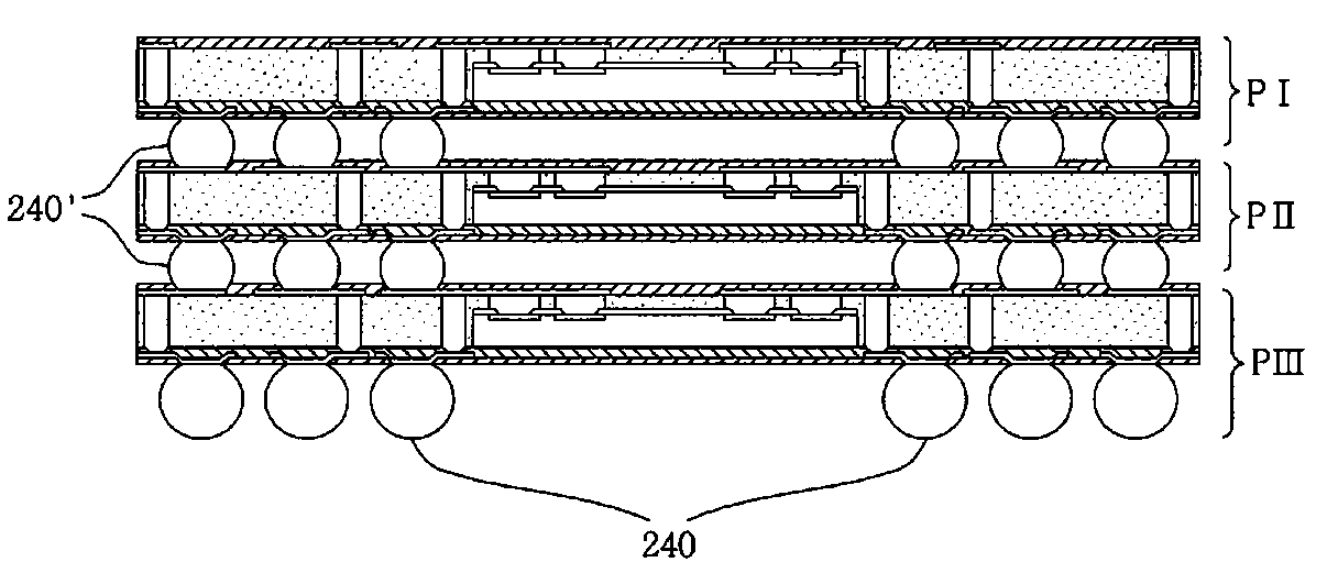
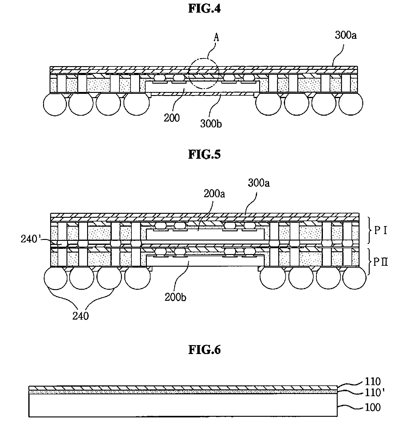
[0030]The semiconductor chip 200 is electrically connected to conductive structures 140, each formed in a post shape at one side of the multilayer thin film layer, through the redistribution layer 120, and the semiconductor chip 200 is finally electrically connected to solder bumps 240 for external connection, which are electrically connected to the conductive structures 140. The con...
second embodiment
[0061]Likewise, in the semiconductor package the conductive structures 140 formed at one side of the multilayer thin film layer and the semiconductor chip 200′ are partially covered by a molding part 150, and the multilayer thin film layer and the molding part 150 physically support the semiconductor chip 200′, to form one package structure.
[0062]The semiconductor chip 200′ directly attached on the multilayer thin film layer is of a face-up type. A part of the multilayer thin film layer formed at the bottom side of the semiconductor chip 200′ may be removed to be exposed to the outside or a thermal conductive sheet may be attached to the multilayer thin film layer, to smoothly spread out the heat from the semiconductor chip 200′.
[0063]Under the multilayer thin film layer, the solder bumps 240 are formed to be electrically connected to the redistribution layer 120. An under bump metal (not shown) may be further included between the redistribution layer 120 and the solder bumps 240. ...
PUM
 Abstract
Description
Claims
Application Information