

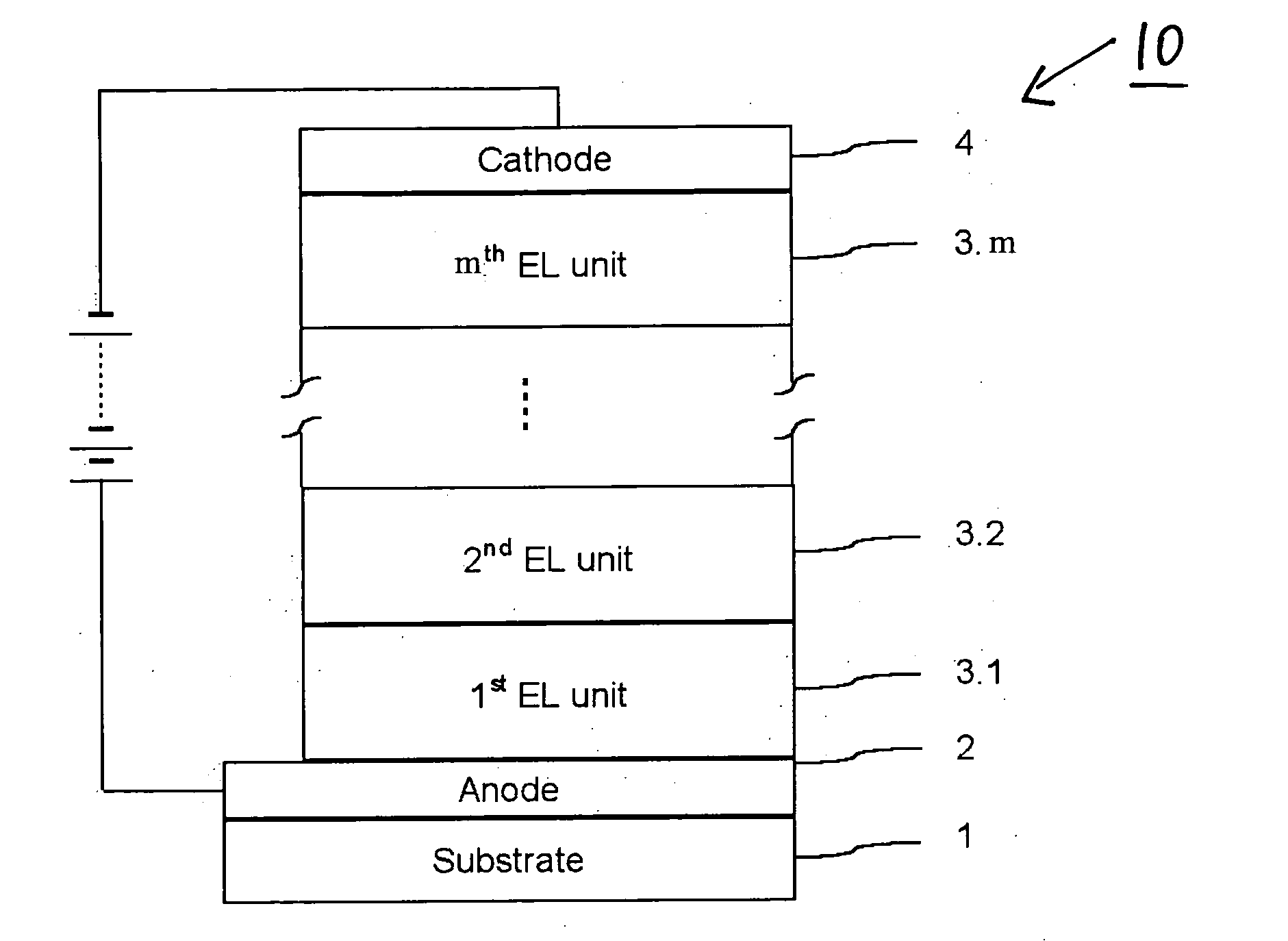
Organic Light Emitting Device With a Plurality of Organic Electroluminescent Units Stacked Upon Each Other
a light-emitting device and organic technology, applied in the direction of discharge tube luminescnet screens, discharge tube/lamp details, electric discharge lamps, etc., can solve the problems of reduced operating voltage of electroluminescent devices, feature extremely low operating voltage, and higher manufacturing costs
- Summary
- Abstract
- Description
- Claims
- Application Information
AI Technical Summary
Problems solved by technology
Method used
Image

Examples
example 1
Reference
[0048]1) 45 nm 2,2′,7,7′-Tetrakis-(N,N-di-methylphenylamino)-9,9′-spirobifluoren doped with 2-(6-Dicyanomethylene-1,3,4,5,7,8-hexafluoro-6H-naphtalen-2-ylidene)-malononitrile (p-HTL);[0049]2) 20 nm 4,4′,4″-tris(N-carbazolyl)-triphenylamine doped with fac-tris(2-phenylpyridine) iridium;[0050]3) 10 nm 1,3,5-tri(phenyl-2-benzimidazole)-benzene doped with fac-tris(2-phenylpyridine) iridium;[0051]4) 40 nm Bathophenantroline doped with Cs (n-ETL); and[0052]5) 100 nm Aluminum as a reflective cathode.
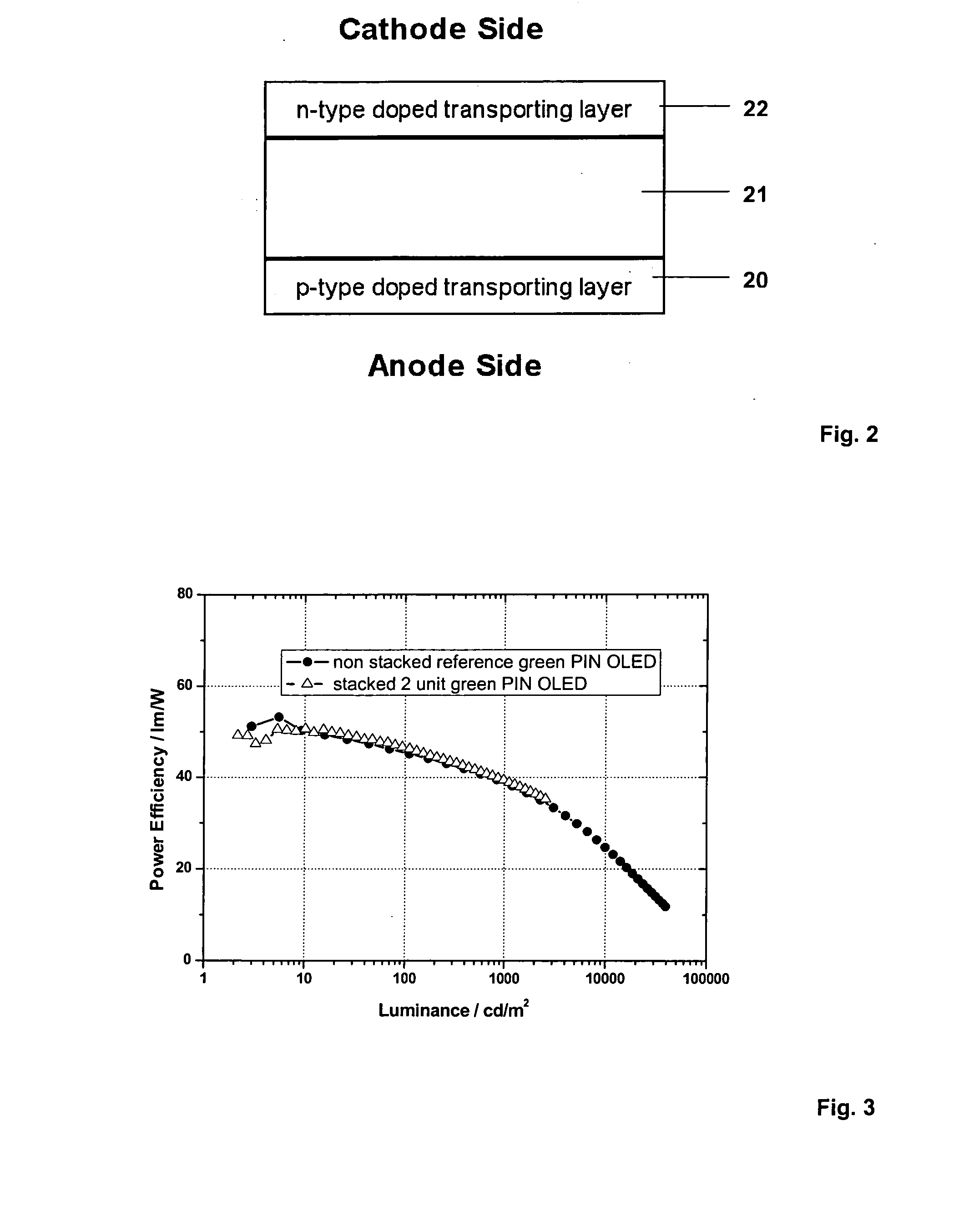
[0053]The EML is made of layers 2), and 3). This is a green phosphorescent PIN OLED having col- or coordinates of 0.29 / 0.64 at a brightness of 1000 cd / m2. This brightness is reached at an operating voltage of 4.15 V, much lower than those without p-type doped hole-transporting layers and n-type doped electron-transporting layers. At a brightness of 1000 cd / m2 the current efficiency of the device is 51.3 cd / A. The power efficiency at this brightness is 38.8 lM / W.
example 2
Stacked Electroluminescent Units
[0054]1) 45 nm 2,2′,7,7′-Tetrakis-(N,N-di-methylphenylamino)-9,9′-spirobifluoren doped with 2-(6-Dicyanomethylene-1,3,4,5,7,8-hexafluoro-6H-naphtalen-2-ylidene)-malononitrile (p-HTL);[0055]2) 20 nm 4,4′,4″-tris(N-carbazolyl)-triphenylamine doped with fac-tris(2-phenylpyridine) iridium;[0056]3) 10 nm 1,3,5-tri(phenyl-2-benzimidazole)-benzene doped with fac-tris(2-phenylpyridine) iridium;[0057]4) 40 nm Bathophenantroline doped with Cs (n-ETL); (1st electroluminescent unit)[0058]5) 95 nm 2,2′,7,7′-Tetrakis-(N,N-di-methylphenylamino)-9,9′-spirobifluoren doped with 2-(6-Dicyanomethylene-1,3,4,5,7,8-hexafluoro-6H-naphtalen-2-ylidene)-malononitrile (p-HTL);[0059]6) 20 nm 4,4′,4″-tris(N-carbazolyl)-triphenylamine doped with fac-tris(2-phenylpyridine) iridium;[0060]7) 10 nm 1,3,5-tri(phenyl-2-benzimidazole)-benzene doped with fac-tris(2-phenylpyridine) iridium;[0061]8) 40 nm Bathophenantroline doped with Cs (n-ETL); (2nd electroluminescent unit)[0062]9) 100 nm...
PUM
 Abstract
Description
Claims
Application Information