
Systems for plasma enhanced chemical vapor deposition and bevel edge etching

a technology of chemical vapor deposition and edge etching, applied in chemical vapor deposition coating, coating, electric discharge tubes, etc., can solve the problems of unsatisfactory edge area and the approach using the shadow ring 105

Active Publication Date: 2009-01-15
APPLIED MATERIALS INC
View PDF17 Cites 160 Cited by
  • Summary
  • Abstract
  • Description
  • Claims
  • Application Information

AI Technical Summary

Benefits of technology

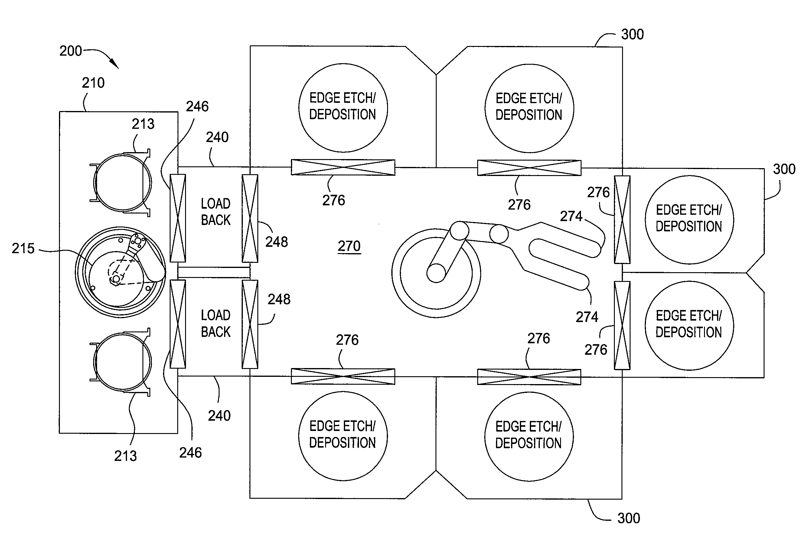
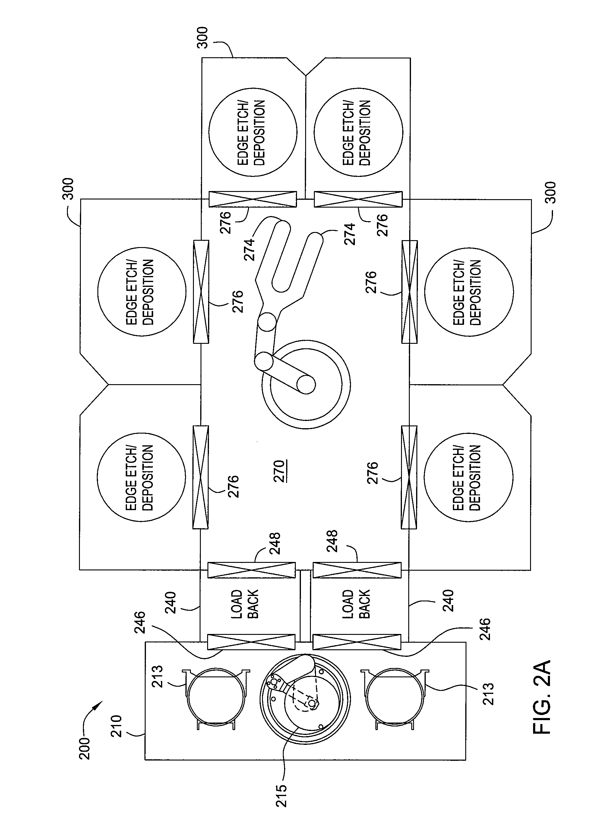
[0010]The present application describes substrate processing apparatuses and methods that integrate substrate edge processing capabilities. In one embodiment, an apparatus comprises a loadlock chamber, a transfer chamber coupled to the loadlock chamber, and one or more twin process chamber coupled to the transfer chamber, each process chamber defining a plurality of separate processing regions. Each processing region comprises a substrate support having a substrate support surface, a plasma generator configured to supply an etching agent in a plasma phase to a peripheral region of the substrate support surface, and a gas delivery assembly coupled to a gas source, wherein the gas delivery assembly is configured to generate a radial gas flow over the substrate support surface, and the radial gas flow travels from an approximately central region of the substrate support surface toward the peripheral region of the s

Problems solved by technology

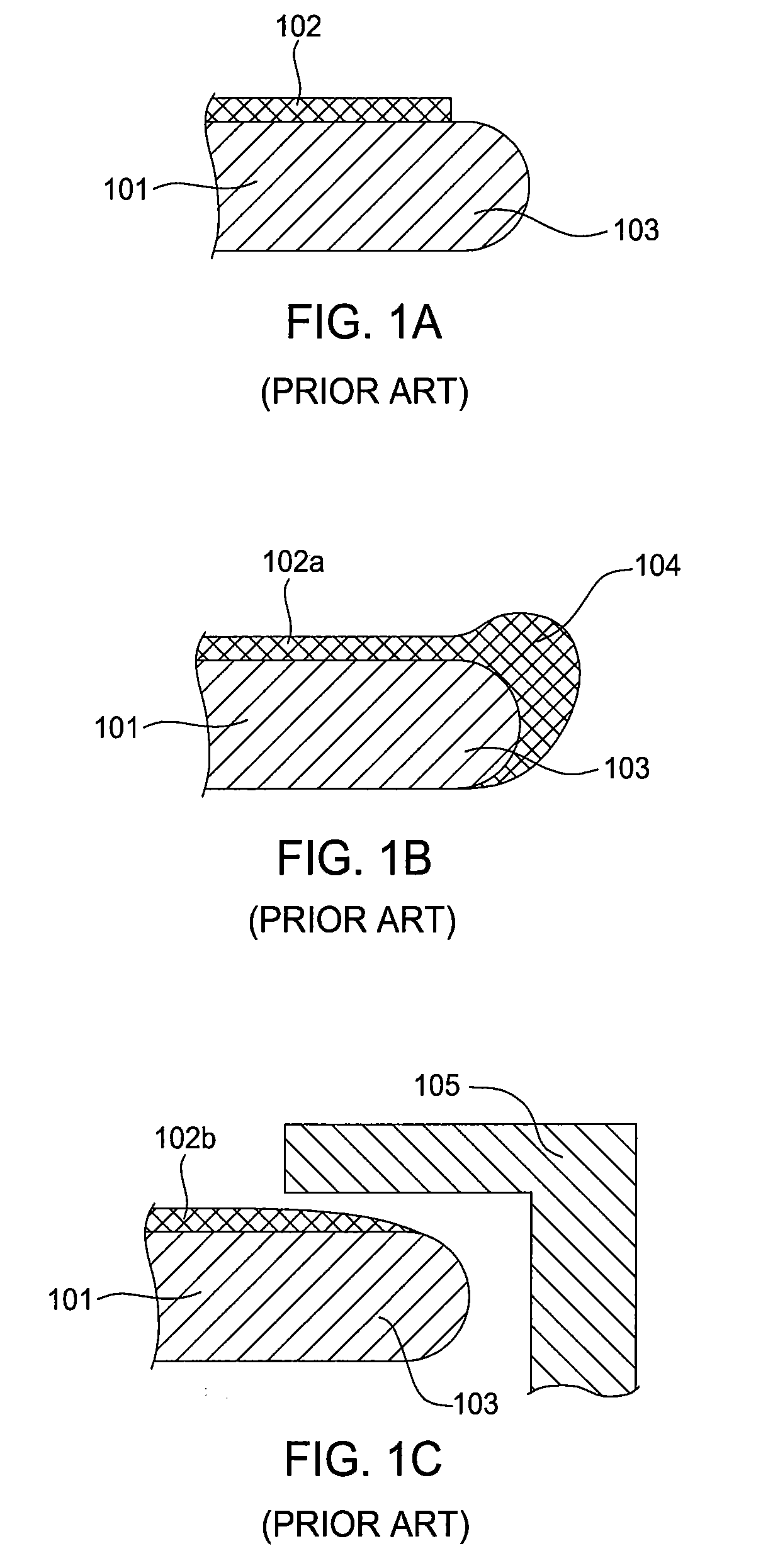
As a result of the smaller edge exclusion area, the conventional approach using the shadow ring 105 to prevent deposition at the edge area may not provide satisfactory result.

Method used


Image

  • Systems for plasma enhanced chemical vapor deposition and bevel edge etching
  • Systems for plasma enhanced chemical vapor deposition and bevel edge etching
  • Systems for plasma enhanced chemical vapor deposition and bevel edge etching

Examples


Embodiment Construction

[0029]Embodiments described herein relate to a substrate processing system that integrates substrate edge processing capabilities. More specifically, the processing system is operable to receive the load of one or more substrate, form a deposition film on each substrate, and etch a selective portion of the deposition film at an edge region of the substrate. Illustrated examples of the processing system comprises, without limitations, a factory interface, a loadlock chamber, a transfer chamber, and one or more twin process chambers having two or more processing regions that are isolatable from each other and share a common gas supply and a common exhaust pump. The processing regions in each twin process chamber include separate gas distribution assemblies and RF power sources to provide plasma at selective regions on a substrate surface in each processing region. Each twin process chamber is thereby configured to allow multiple, isolated processes to be performed concurrently on at l...


PUM

PropertyMeasurementUnit
Distanceaaaaaaaaaa
Processing propertiesaaaaaaaaaa

Abstract

Embodiments described herein relate to a substrate processing system that integrates substrate edge processing capabilities. Illustrated examples of the processing system include, without limitations, a factory interface, a loadlock chamber, a transfer chamber, and one or more twin process chambers having two or more processing regions that are isolatable from each other and share a common gas supply and a common exhaust pump. The processing regions in each twin process chamber include separate gas distribution assemblies and RF power sources to provide plasma at selective regions on a substrate surface in each processing region. Each twin process chamber is thereby configured to allow multiple, isolated processes to be performed concurrently on at least two substrates in the processing regions.

Description

CROSS-REFERENCE TO RELATED APPLICATIONS[0001]This application claims the benefit of U.S. Provisional Patent Applications Ser. No. 60 / 949,397 (Attorney Docket No. 011997L), filed Jul. 12, 2007, Ser. No. 60 / 982,961 (Attorney Docket No. 011997L02), filed Oct. 26, 2007, and Ser. No. 60 / 982,993 (Attorney Docket No. 011997L03), filed Oct. 26, 2007. All aforementioned patent applications are herein incorporated by reference.BACKGROUND OF THE INVENTION[0002]1. Field of the Invention[0003]Embodiments of the invention generally relate to apparatus and methods for processing semiconductor substrates. More particularly, embodiments of the present invention relate to apparatus and methods for processing a substrate near an edge region.[0004]2. Description of the Related Art[0005]To reduce the cost of ownership, semiconductor manufacture processes may be performed in an integrated system that is capable of processing multiple substrates in parallel with high repeatability. The integrated system u...

Claims


Application Information

Patent Timeline
IPC IPC(8): C23F1/02
CPCH01J37/32366H01J2237/3321H01L21/67207H01L21/67201H01L21/6719
Inventor SHAH, ASHISHDUBOIS, DALE R.BALASUBRAMANIAN, GANESHFODOR, MARK A.KIM, EUI KYOONCHAN, CHIUJANAKIRAMAN, KARTHIKNOWAK, THOMASWERNER, JOSEPH C.SIVARAMAKRISHNAN, VISWESWARENAYOUB, MOHAMADAL-BAYATI, AMIRZHOU, JIANHUA
Owner APPLIED MATERIALS INC
Learn More