Low skew clock distribution tree

a clock distribution and low skew technology, applied in the field of integrated circuit memory, can solve the problems of loss of clock and data performance, unmatched widths and spacings of various clock busses and clock bus segments, and increasing clock and signal skew, so as to maximize valid times and minimize clock skew.

Inactive Publication Date: 2009-01-15
SONY CORP
View PDF4 Cites 0 Cited by
  • Summary
  • Abstract
  • Description
  • Claims
  • Application Information

AI Technical Summary

Benefits of technology

[0008]According to the present invention, a clock distribution tree for an integrated circuit memory includes a plurality of data drivers, a plurality of input buffers coupled to the plurality of data drivers, a first clock distribution tree coupled to the plurality of data drivers, and a second clock distribution tree coupled to the plurality of input buffers, wherein the first and second clock distribution tree are substantially matched and mirrored distribution trees. The line width of the first clock distribution tree is substantially the same as the line width of the second clock distribution tree. The line spacing of the first clock distribution tree is substantially the same as the line spacing of the second clock distribution tree. Numerous topologies for the first and second clock distribution trees can be accommodated, as long as they are matched and mirrored. According to the present invention, valid times are maximized and data and clock skew is minimized.

Problems solved by technology

Clock and signal skew are becoming larger as chip sizes increase.
Further, the widths and spacings associated with the various clock busses and clock bus segments is also unmatched.
This leads to clock and data skew and loss of performance.
So even though this is a better design to reduce skew, it is inferior in maximizing the valid data window for these buffers.

Method used


Image

  • Low skew clock distribution tree
  • Low skew clock distribution tree
  • Low skew clock distribution tree

Examples


first embodiment

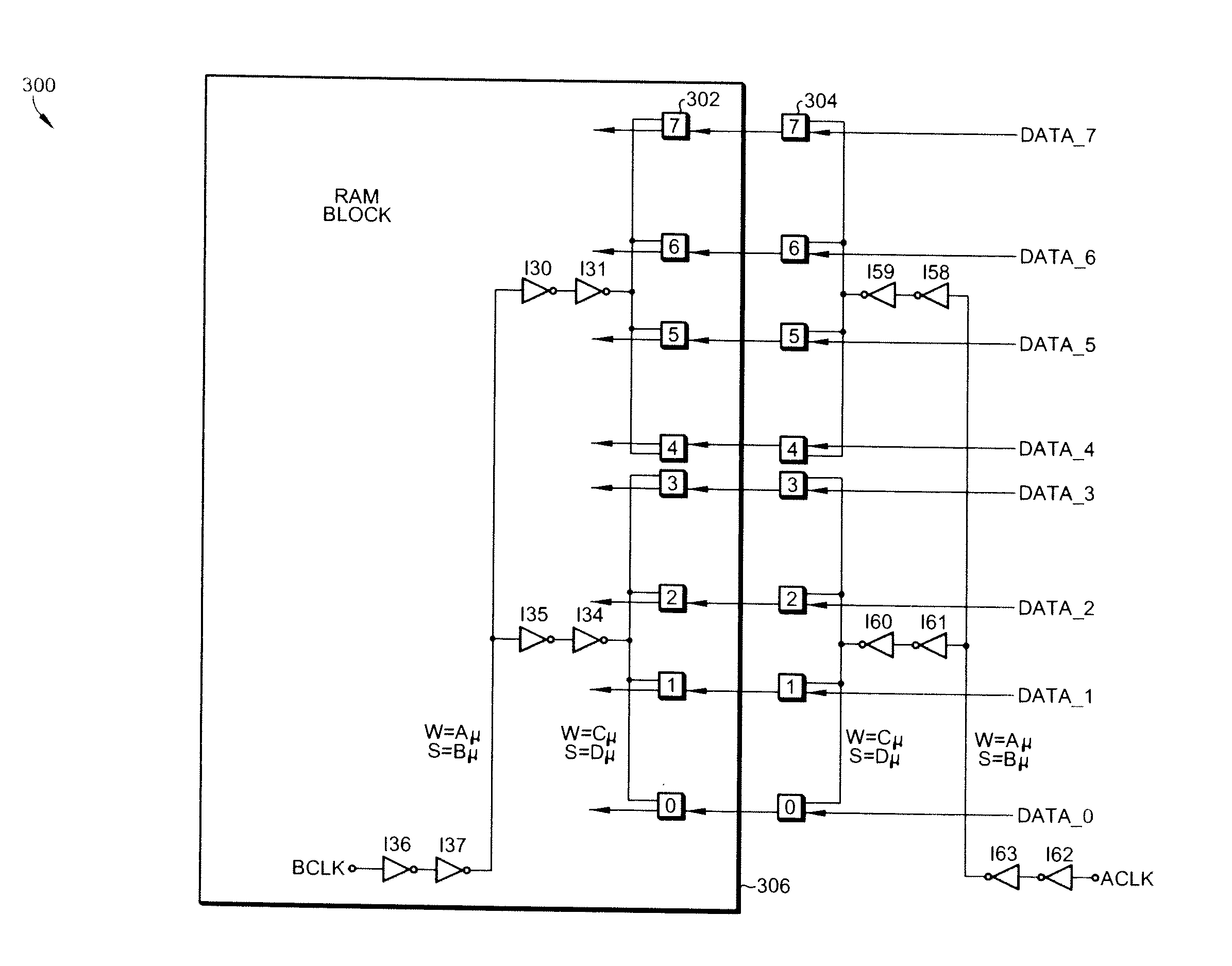
[0018]A clock distribution tree circuit is shown for a portion of an integrated circuit memory 300 in FIG. 3 according to the present invention. Integrated circuit memory 300 includes input buffers 302 designated 0 through 7 resident in RAM block 306. Each input buffer has a data input, a data output, and a clock input. Integrated circuit memory 300 also includes data drivers 204 designated 0 through 7, corresponding to each of the input buffers. The clock input, data input, and the data output of the data drivers 304 are all shown in FIG. 3. The data drivers 304 are clocked by a first clock distribution tree including inverters I59-I63. Inverters I58 and I59 clock data drivers 4 through 7 and inverters I60 and I61 clock data drivers 0 through 3. In turn, inverters I62 and I63 drive inverters I58 and I61. The input buffers 302 are clocked by a second clock distribution tree mirroring the first clock distribution tree according to an aspect of the present invention including inverter...

second embodiment

[0020]A clock distribution tree circuit is shown for a portion of an integrated circuit memory 400 in FIG. 4 according to the present invention. Integrated circuit memory 400 includes input buffers 402 designated 0 through 7 resident in RAM block 406. Each input buffer has a data input, a data output, and a clock input. Integrated circuit memory 400 also includes data drivers 404 designated 0 through 7, corresponding to each of the input buffers. The clock input, data input, and the data output of the data drivers 404 are all shown in FIG. 4. The data drivers 404 are clocked by a first clock distribution tree including inverters I58-I59 and I62-I63. The input buffers 402 are clocked by a second clock distribution tree mirroring the first clock distribution tree according to an aspect of the present invention including inverters I30-I31 and I36-I37. Inverter I62 receives the ACLK clock signal, and inverter I36 receives the BCLK signal. The width W (Aμ) and spacings S (Bμ) of the firs...


PUM


Abstract

A clock distribution tree for an integrated circuit memory includes a set of data drivers, a corresponding set of input buffers coupled to the data drivers, a first clock distribution tree coupled to the data drivers, and a second clock distribution tree coupled to the input buffers, wherein the first and second clock distribution tree are substantially matched and mirrored distribution trees. The line width of the first clock distribution tree is substantially the same as the line width of the second clock distribution tree. The line spacing of the first clock distribution tree is substantially the same as the line spacing of the second clock distribution tree. Numerous topologies for the first and second clock distribution trees can be accommodated, as long as they are matched and mirrored. Valid times for the integrated circuit memory are maximized and data and clock skew is minimized.

Description

BACKGROUND OF THE INVENTION[0001]The present invention is related to integrated circuit memories, and, more particularly, to a clock distribution tree for minimizing data skew between data drivers and associated input buffers in the memory.[0002]Capture windows for inputs and outputs on today's high speed memories are becoming smaller. Input set up times (tS) and hold times (tH) are reduced as clock frequencies increase. Clock and signal skew are becoming larger as chip sizes increase. Because of these two trends, higher speed systems and larger chip size or RAM macro size, the actual valid time is being reduced for inputs and outputs to RAM circuit blocks.[0003]Typical clock distribution trees 100 are shown in FIGS. 1(a)-1(d). There are many different ways to distribute or route a clock or control signal around a silicon integrated circuit. These many different ways of routing have different skew values or time differences between the closest (fastest) location and the furthest (sl...

Claims


Application Information

Patent Timeline
Patent Type & Authority Applications(United States)
IPC IPC(8): H03K3/84
CPCG06F1/10G11C5/063G11C7/1051G11C7/1057G11C11/4093G11C7/1084G11C7/22G11C7/222G11C11/4076G11C7/1078
Inventor PARRIS, MICHAEL C.JONES, JR., OSCAR FREDERICK
Owner SONY CORP
Why Eureka
Try Eureka