Semiconductor device

a technology of semiconductors and devices, applied in the direction of semiconductor devices, electrical devices, transistors, etc., can solve the problems of reducing the efficiency of semiconductor devices, so as to achieve stable operation

Active Publication Date: 2009-01-22
MITSUBISHI ELECTRIC CORP
View PDF2 Cites 51 Cited by
  • Summary
  • Abstract
  • Description
  • Claims
  • Application Information

AI Technical Summary

Benefits of technology

[0014]An object of the present invention is to provide a semiconductor device having a trench

Problems solved by technology

However, as discussed in Document 1, there is raised a trade-off problem concerning optimization of on-voltage and saturation current.
Further, when the emitter region is formed in stripes, a problem described below is also raised, although it is not discussed in Document 1.
When the emitter region is narrow in width, a large voltage is applied across a junction between the emitter and the base and breaks down the junction, which leads to element breakdown and raises a problem of narrowing

Method used


Image

  • Semiconductor device
  • Semiconductor device
  • Semiconductor device

Examples


first embodiment

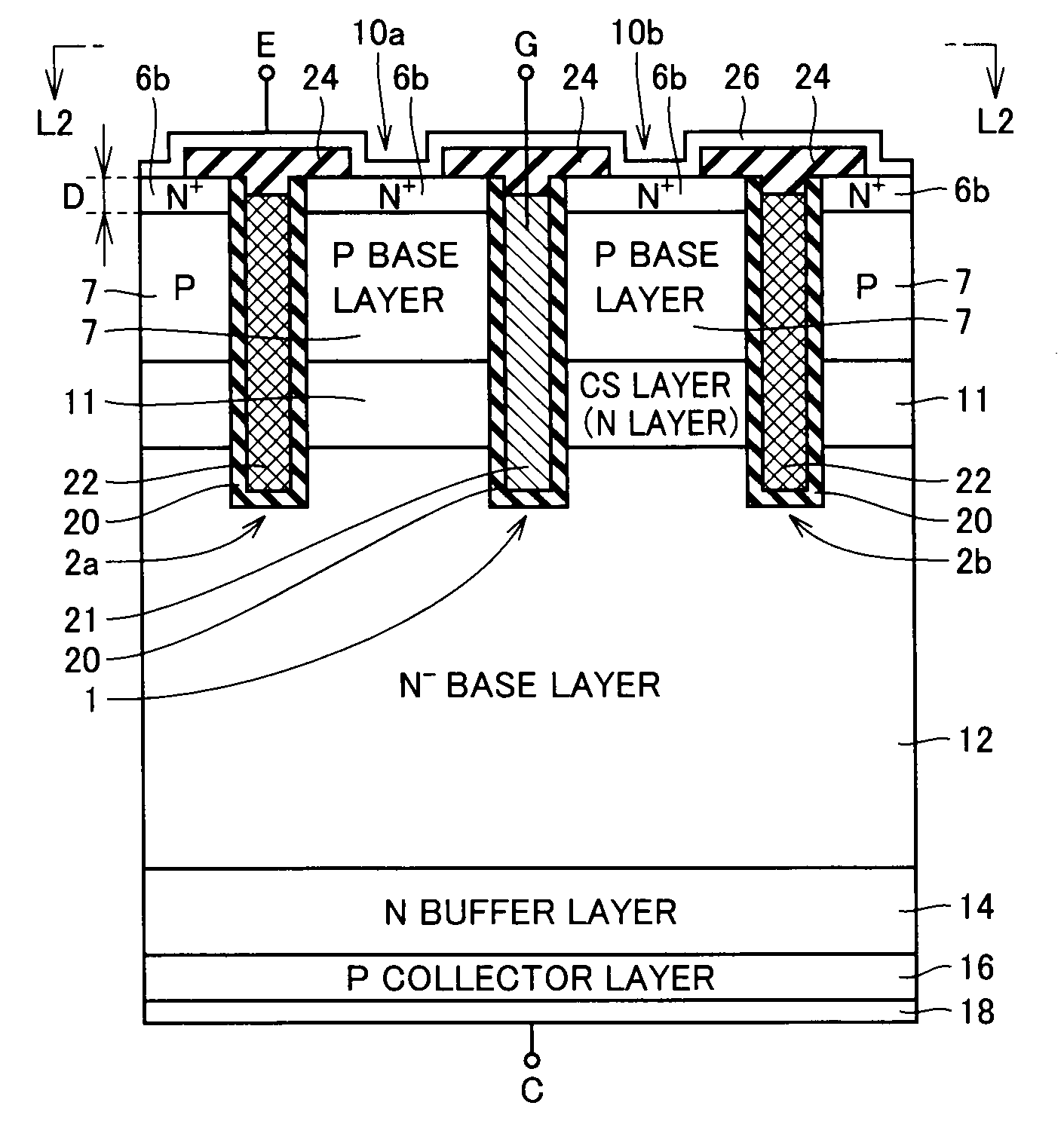
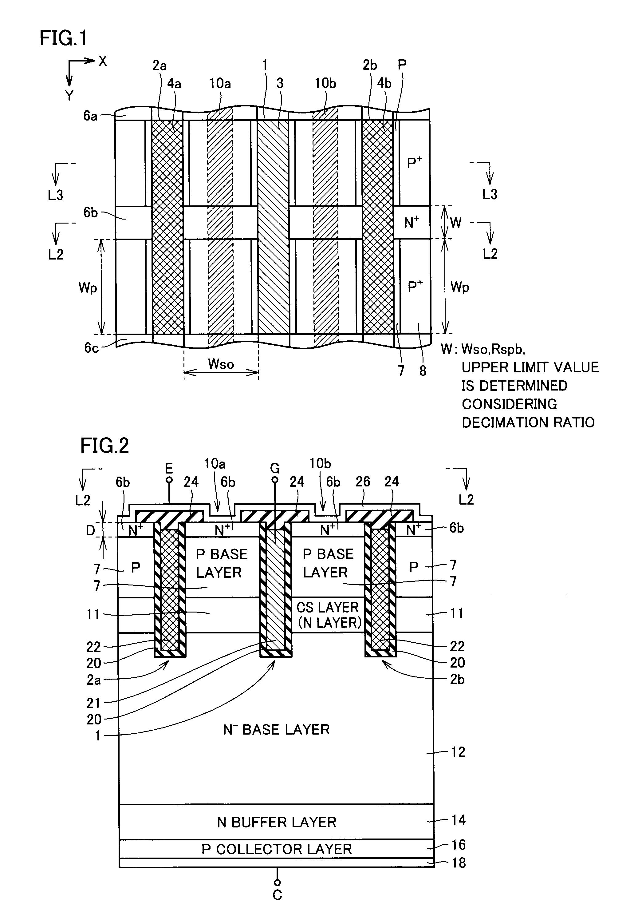
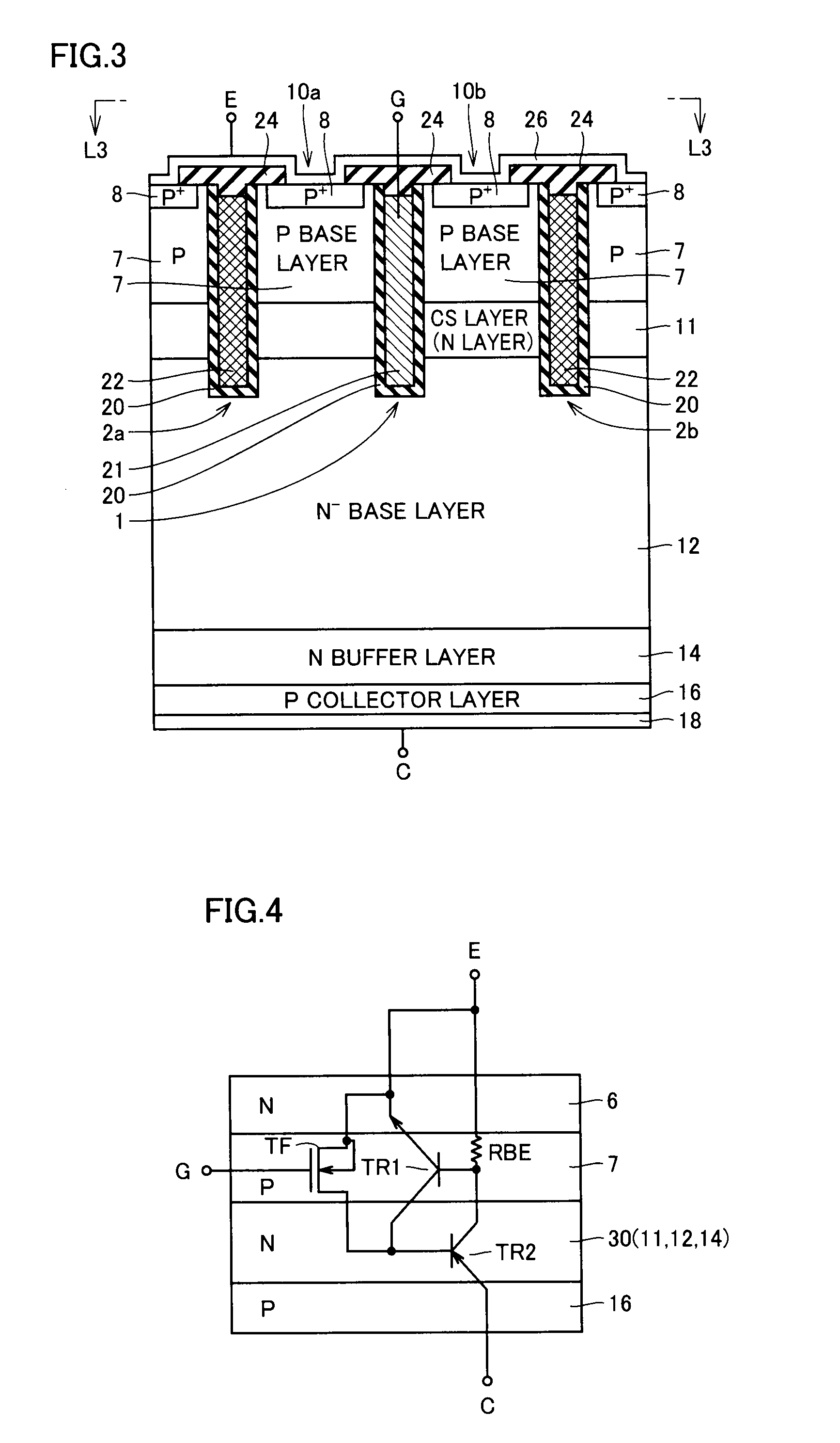
[0038]FIG. 1 schematically shows a surface layout of an IGBT in accordance with a first embodiment of the present invention. In FIG. 1, an emitter electrode is not shown for brevity of the drawing.

[0039]In FIG. 1, trench regions 1, 2a, and 2b are provided linearly extending in a Y direction and being spaced from each other in an X direction. A gate electrode layer 3 is formed in trench region 1, and insulating materials 4a and 4b are deposited on inner walls of trench regions 2a and 2b, respectively. Trench regions 2a and 2b do not serve as gate electrodes, and are provided to narrow an ejection path for minority carriers (holes) to increase ejection resistance to the minority carriers (holes: hereinafter simply referred to as holes) for accumulating the holes.

[0040]Gate electrode layer 3 in trench region 1 forms a channel along a side wall of trench region 1 according to a voltage applied to gate electrode layer 3, and serves as an effective gate of a semiconductor device. In the d...


PUM


Abstract

An emitter layer is provided in stripes in a direction orthogonal to an effective gate trench region connected to a gate electrode and a dummy trench region isolated from the gate electrode. A width of the emitter layer is determined to satisfy a predetermined relational expression so as not to cause latch-up in an underlying P base layer. In the predetermined relational expression, an upper limit value of the width W of the emitter layer is (3500/Rspb)·Wso·exp(decimation ratio), where Rspb is a sheet resistance of the P base layer immediately below the emitter layer, Wso is an interval between the trenches, and the decimation ratio is a ratio of the number of the effective gate trench region to the total number of the trench regions. Variations in saturation current in a trench IGBT can be suppressed, and a tolerance of an Reverse Bias Safe Operation Area can be improved.

Description

BACKGROUND OF THE INVENTION[0001]1. Field of the Invention[0002]The present invention relates to a semiconductor device, and in particular to a power semiconductor device for driving high power. More specifically, the present invention relates to a structure for suppressing variations in saturation current in an IGBT (Insulated Gate Bipolar Transistor) having a trench gate structure.[0003]2. Description of the Background Art[0004]Power transistors are widely used for power conversion or control. One type of such power transistors is an insulated gate bipolar transistor (IGBT). The IGBT generally has an emitter layer of a first conductivity type, a base layer of a second conductivity type, a drift layer (base layer) of the first conductivity type, a collector layer of the second conductivity type, and a gate electrode formed facing the base layer and the drift layer with an insulating film interposed in between. A channel is formed in the base layer by applying a voltage to the gate ...

Claims


Application Information

Patent Timeline
IPC IPC(8): H01L29/739
CPCH01L29/7397H01L29/0696H01L29/73H01L29/70
Inventor HARADA, TATSUO
Owner MITSUBISHI ELECTRIC CORP
Why Eureka
Try Eureka