Thin film transistor array substrate and method for manufacturing the same

a technology of thin film transistors and array substrates, applied in the direction of electrical equipment, semiconductor devices, instruments, etc., can solve the problems of line cutting and shutdown crosstalk, and achieve the effects of preventing defects, reducing resistance, and improving aperture ratio

Active Publication Date: 2009-01-29
LG DISPLAY CO LTD
View PDF3 Cites 17 Cited by
  • Summary
  • Abstract
  • Description
  • Claims
  • Application Information

AI Technical Summary

Benefits of technology

[0021]An object of the present invention is to provide a thin film transistor array substrate which has a “U”-shaped common line formed in a pixel region in order to improve an aperture ratio, and

Problems solved by technology

If a line width of the common line is reduced or a shape of the common line is changed in order to prevent the loss of an

Method used


Image

  • Thin film transistor array substrate and method for manufacturing the same
  • Thin film transistor array substrate and method for manufacturing the same
  • Thin film transistor array substrate and method for manufacturing the same

Examples


Embodiment Construction

[0036]Reference will now be made in detail to the preferred embodiments of the present invention associated with a thin film transistor array substrate and a method for manufacturing the same, examples of which are illustrated in the accompanying drawings. Wherever possible, the same reference numbers will be used throughout the drawings to refer to the same or like parts.

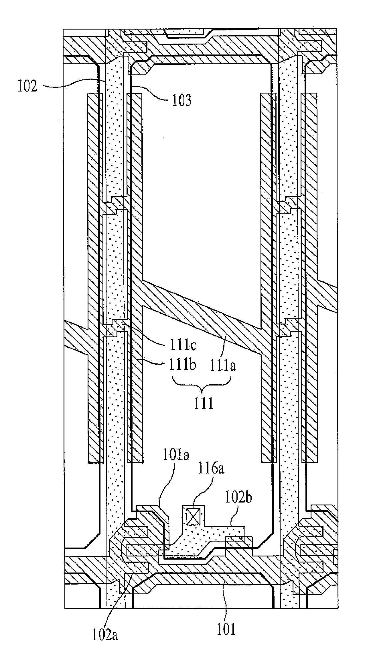
[0037]FIG. 3 is a plan view illustrating a thin film transistor array substrate according to an exemplary embodiment of the present invention, and FIG. 4 is a sectional view taken along line II-II′ of FIG. 3.

[0038]As shown in FIGS. 3 and 4, a thin film transistor array substrate according to the present invention includes a plurality of gate lines 301 and a plurality of data lines 302 intersecting each other to define pixel regions on the substrate 300, thin film transistors (TFTs) formed at the intersections of the gate lines 301 and the data lines 302, and pixel electrodes 303 formed in the pixel regions. The pix...


PUM


Abstract

A thin film transistor array substrate and a method for manufacturing the same are disclosed. The thin film transistor array substrate includes a plurality of gate lines and a plurality of data lines on a substrate, to define pixel regions crossing each other, thin film transistors, each formed at the intersection of the gate lines and the data lines, and including a gate electrode, a source electrode and a drain electrode, common lines, each including a first pattern formed across the data lines, a second pattern formed adjacent to the data lines on both sides in the pixel region and parallel to the data lines, and a third pattern formed adjacent to the gate lines to connect the second pattern disposed on both the sides in the associated one of the pixel regions, and passing below the drain electrode of the thin film transistors and pixel electrodes formed in the pixel regions.

Description

[0001]This application claims the benefit of Korean Patent Application No. 10-2007-074723, filed on Jul. 25, 2007, which is hereby incorporated by reference as if fully set forth herein.BACKGROUND OF THE INVENTION[0002]1. Field of the Invention[0003]The present invention relates to a liquid crystal display device, and more particularly, to a thin film transistor array substrate and a method for manufacturing the same, which has a “U”-shaped common line formed in a pixel region in order to improve an aperture ratio, and can decrease a resistance by increasing a line width of the common line from a region near a thin film transistor to a region below a drain electrode and can prevent defects such as line cut, etc.[0004]2. Discussion of the Related Art[0005]With the progress of an information-dependent society, the demand for various display devices has increased. To meet such a demand, efforts have recently been made to research flat panel display devices such as liquid crystal displa...

Claims


Application Information

Patent Timeline
IPC IPC(8): H01L27/12H01L21/70
CPCG02F1/136213G02F1/136227H01L27/124G02F2201/40G02F2001/136218G02F1/136218G02F1/134309G02F1/136286H01L27/12H01L27/1214
Inventor SHIN, KI TAEGCHO, SUNG HYUNPARK, TAE JOON
Owner LG DISPLAY CO LTD
Why Eureka
Try Eureka