Pixel, organic light emitting display using the same, and associated methods

a technology of organic light and display, applied in the field of pixels and organic light emitting display, can solve problems such as difficulty in providing such uniform operation

Active Publication Date: 2009-01-29
SAMSUNG DISPLAY CO LTD
View PDF12 Cites 57 Cited by
  • Summary
  • Abstract
  • Description
  • Claims
  • Application Information

AI Technical Summary

Problems solved by technology

However, providing such uniform operation may be difficult.

Method used


Image

  • Pixel, organic light emitting display using the same, and associated methods
  • Pixel, organic light emitting display using the same, and associated methods
  • Pixel, organic light emitting display using the same, and associated methods

Examples


first embodiment

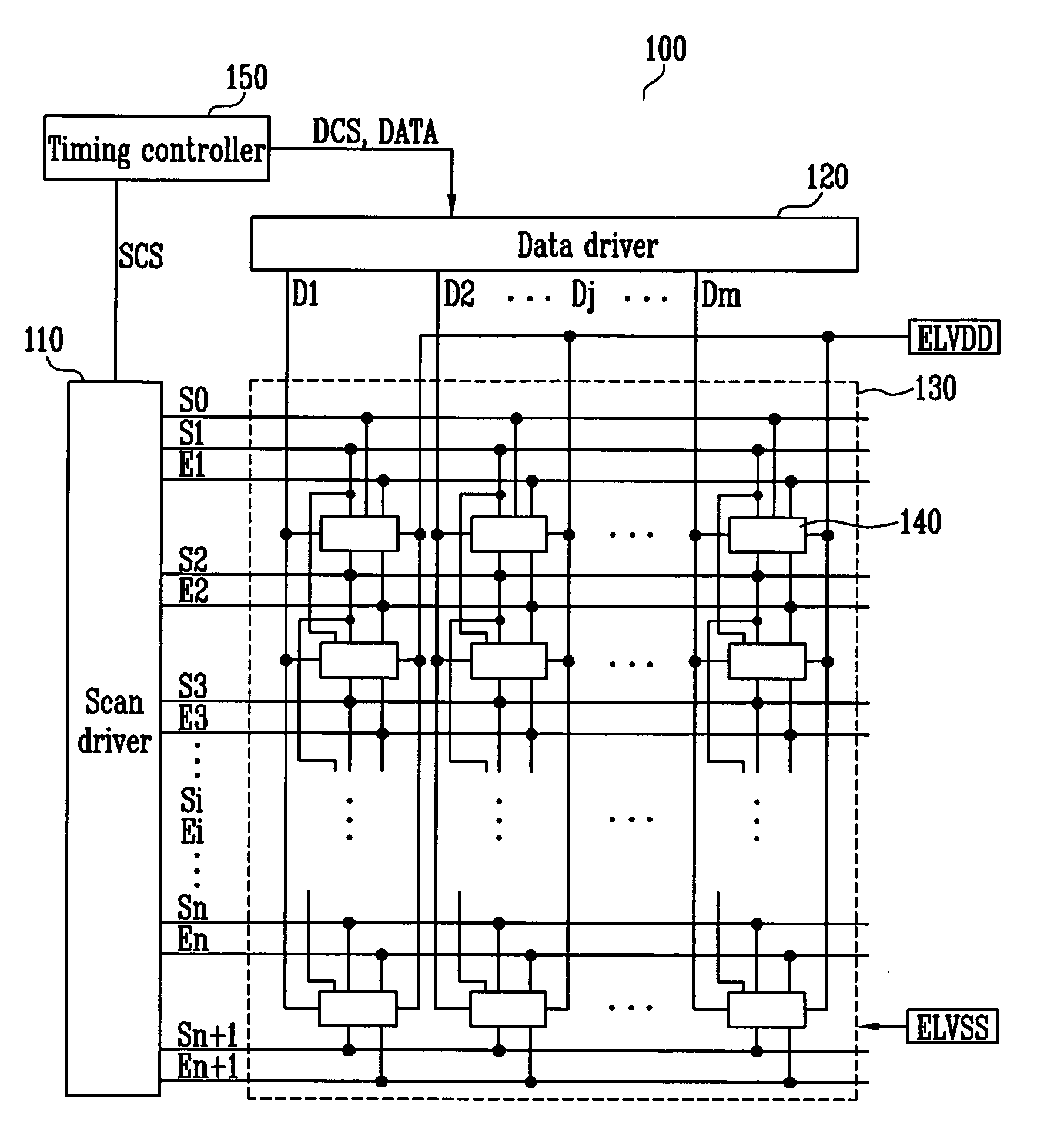
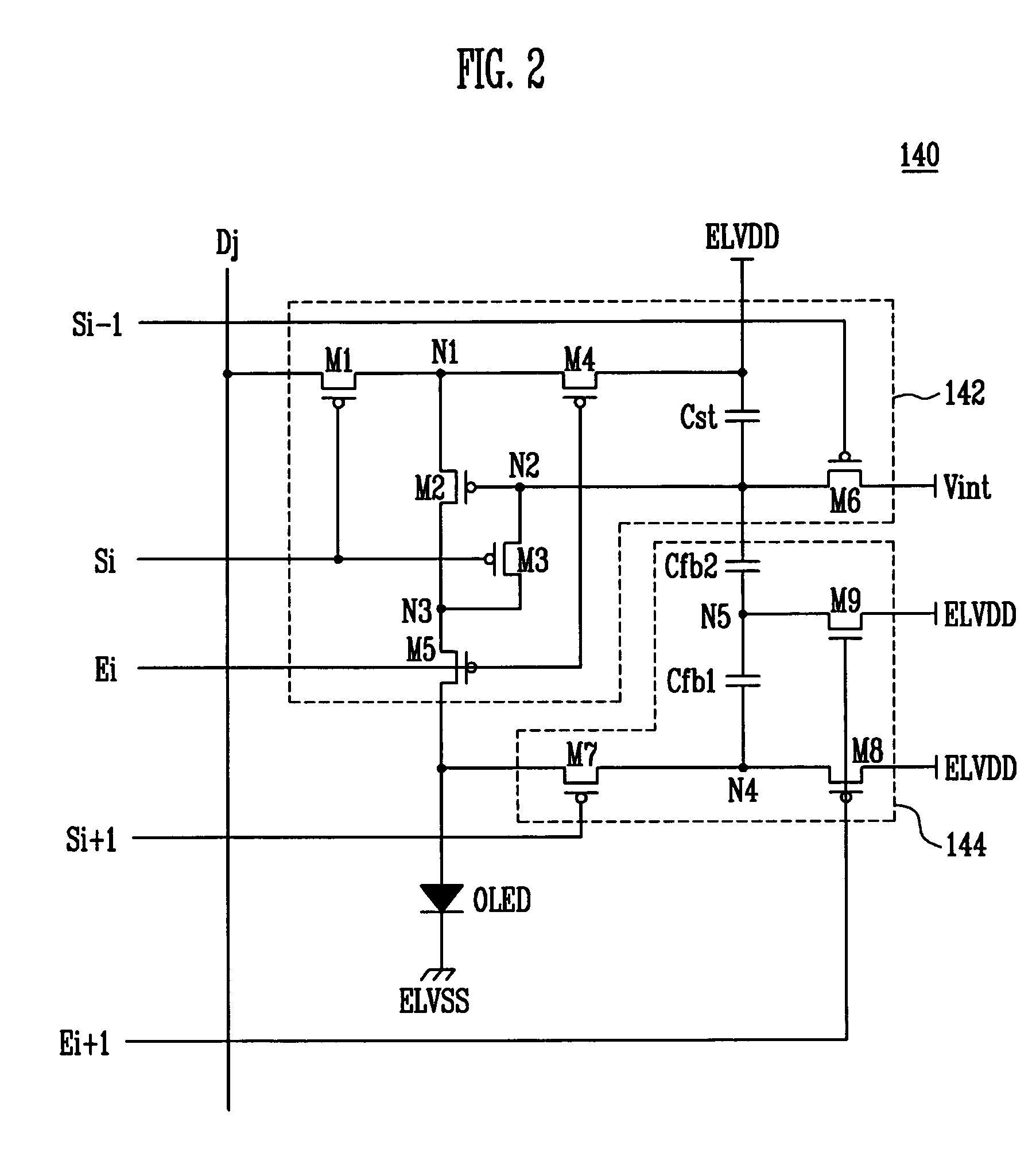
[0036]Referring to FIG. 2, the pixels 140 may include an organic light emitting diode (OLED), the pixel circuit 142 that compensates for the threshold voltage of a second transistor M2 (driving transistor) supplying current to the organic light emitting diode (OLED), and the compensating unit 144 that compensates for the deterioration of the organic light emitting diode (OLED). The compensating unit 144 may control the voltage of a second node N2 coupled to a gate electrode of the second transistor M2 by lowering the voltage as the organic light emitting diode (OLED) deteriorates, in order to compensate for the deterioration of the organic light emitting diode (OLED).

[0037]An anode electrode of the organic light emitting diode (OLED) may be coupled to the pixel circuit 142, and a cathode electrode of the organic light emitting diode (OLED) may be coupled to the second power source ELVSS. The organic light emitting diode (OLED) may generate a predetermined brightness of light corres...

second embodiment

[0063]FIG. 4 illustrates a schematic view of a pixel 140′ according to a For convenience of explanation, FIG. 4 illustrates a pixel 140′ positioned at the ith horizontal line and coupled to the jth data line (Dj).

[0064]The pixel 140′ may be similar to the pixel 140 described above. In particular, the pixel 140′ may include the pixel circuit 142, which may be coupled to light emitting control line Ei, scan lines Si−1 and Si, and data line Dj, in the same manner as the pixel circuit 142 described above in connection with the first embodiment. The pixel 140′ may also include a compensating unit 144′, which may be similar to the compensation unit 144 described above in connection with the first embodiment, except for the construction of a seventh transistor M7′ and the configuration of the signal lines coupled to the compensation unit 144′. In particular, the compensating unit 144′ may have an NMOS transistor as the seventh transistor M7′, whereas the compensating unit 144 may have a P...


PUM


Abstract

A pixel including an organic light emitting diode, a second transistor controlling a current supplied to the organic light emitting diode, a pixel circuit configured to compensate a threshold voltage of the second transistor; and a compensating unit controlling a voltage of a gate electrode of the second transistor in order to compensate for deterioration of the organic light emitting diode. The compensating unit includes seventh and eighth transistors coupled in series between the organic light emitting diode and a first power source, the seventh and eight transistors being commonly connected to a fourth node therebetween, first and second feedback capacitors coupled in series between the fourth node and a second node, the second node being coupled to the gate electrode of the second transistor, and a ninth transistor coupled between a predetermined voltage source and a fifth node that is common to the first and second feedback capacitors.

Description

BACKGROUND OF THE INVENTION[0001]1. Field of the Invention[0002]Embodiments relate to a pixel, an organic light emitting display using the same, and associated methods, in which degradation of an organic light emitting diode is automatically compensated.[0003]2. Description of the Related Art[0004]In the manufacture and operation of a display, e.g., a display used to reproduce text, images, video, etc., uniform operation of pixel elements of the display is highly desirable. However, providing such uniform operation may be difficult. For example, in some display technologies, e.g., those utilizing electroluminescent elements such as organic light emitting diodes (OLEDs), operational characteristics, e.g., luminance, of the pixel elements may change over time. Accordingly, there is a need for a display adapted to compensate for changes in the operational characteristics of pixel elements.SUMMARY OF THE INVENTION[0005]Embodiments are therefore directed to a pixel, an organic light emit...

Claims


Application Information

Patent Timeline
Patent Type & Authority Applications(United States)
IPC IPC(8): G09G3/30
CPCG09G3/3233G09G2300/0819G09G2320/045G09G2320/043G09G2300/0852G09G3/30G09G3/20G09G3/32H05B33/12
Inventor KIM, YANG-WAN
Owner SAMSUNG DISPLAY CO LTD
Why Eureka
Try Eureka