Substrate Processing Apparatus and Substrate Processing Method

a substrate and processing apparatus technology, applied in the direction of semiconductor/solid-state device testing/measurement, coating, electric heating, etc., can solve the problem of limiting the uniformity of the thickness of the film deposited on the substra

Active Publication Date: 2009-01-29
KOKUSA ELECTRIC CO LTD
View PDF10 Cites 34 Cited by
  • Summary
  • Abstract
  • Description
  • Claims
  • Application Information

AI Technical Summary

Benefits of technology

[0004]An object of the invention is to provide a substrate processing apparatus and a substrate processing method capable of controlling uniformity of the thickness of a film deposited on the substrate.

Problems solved by technology

However, even when the desired average temperature deviation M is achieved, there is a limit of uniformity for the thickness of a film deposited on the substrate.

Method used


Image

  • Substrate Processing Apparatus and Substrate Processing Method
  • Substrate Processing Apparatus and Substrate Processing Method
  • Substrate Processing Apparatus and Substrate Processing Method

Examples


Embodiment Construction

Background of the Invention

[0078]In order to facilitate the understanding of the invention, the background as to how the invention was achieved will be described prior to the description of embodiments.

Semiconductor Processing Apparatus 1

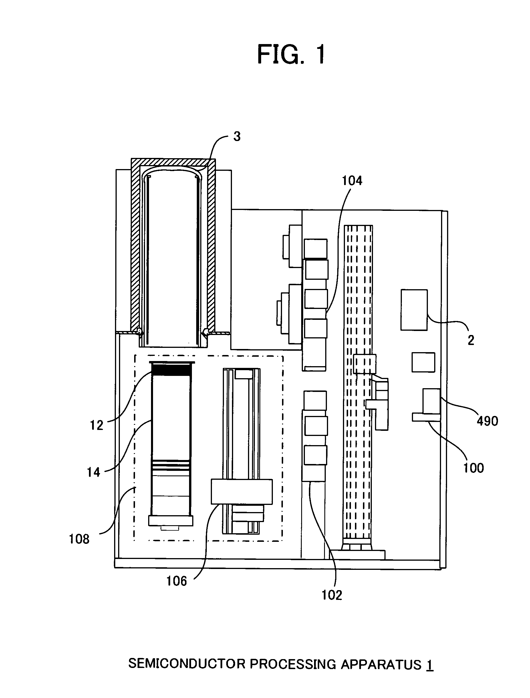
[0079]FIG. 1 is a view showing the overall configuration of a semiconductor processing apparatus 1 to which the invention is applicable.

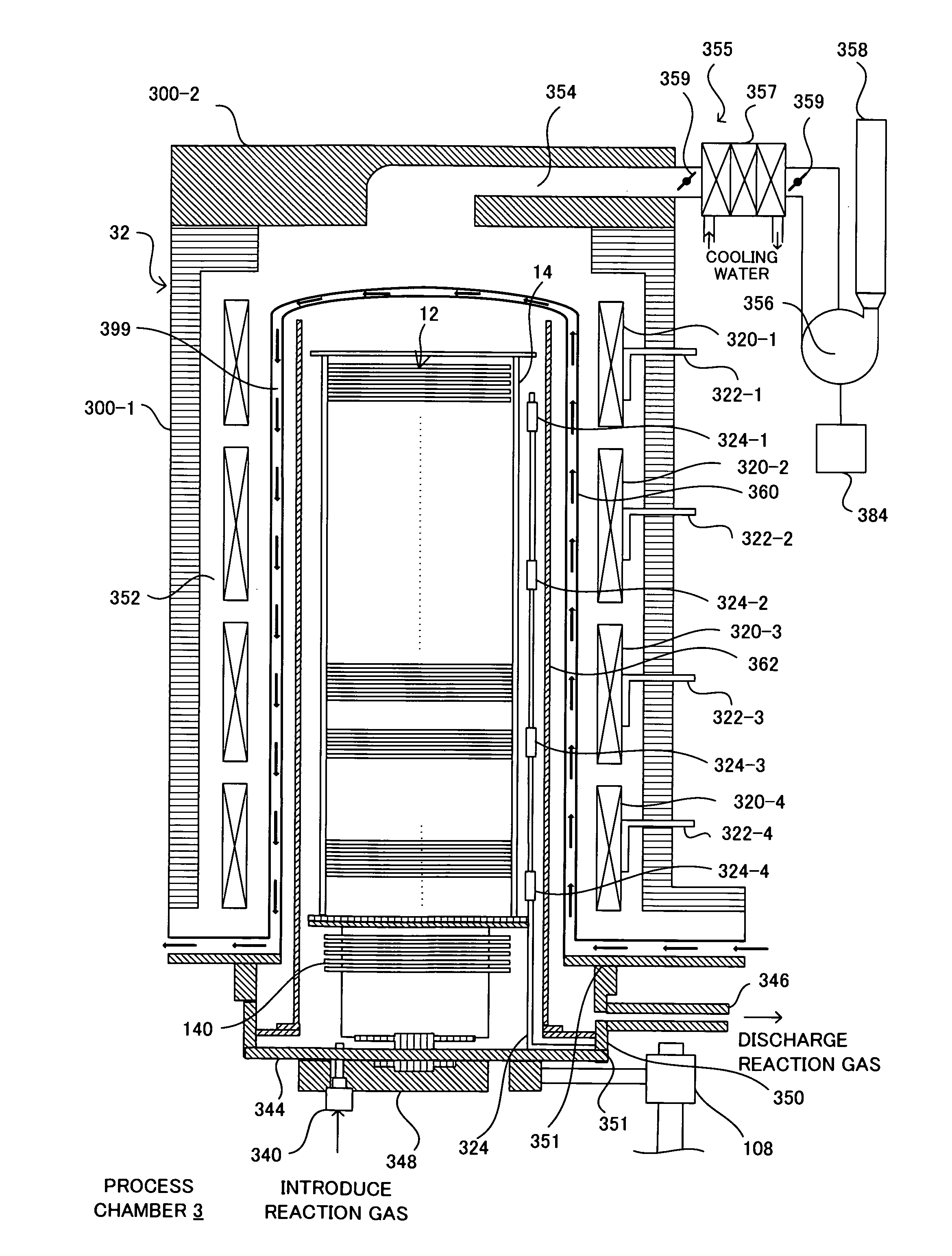
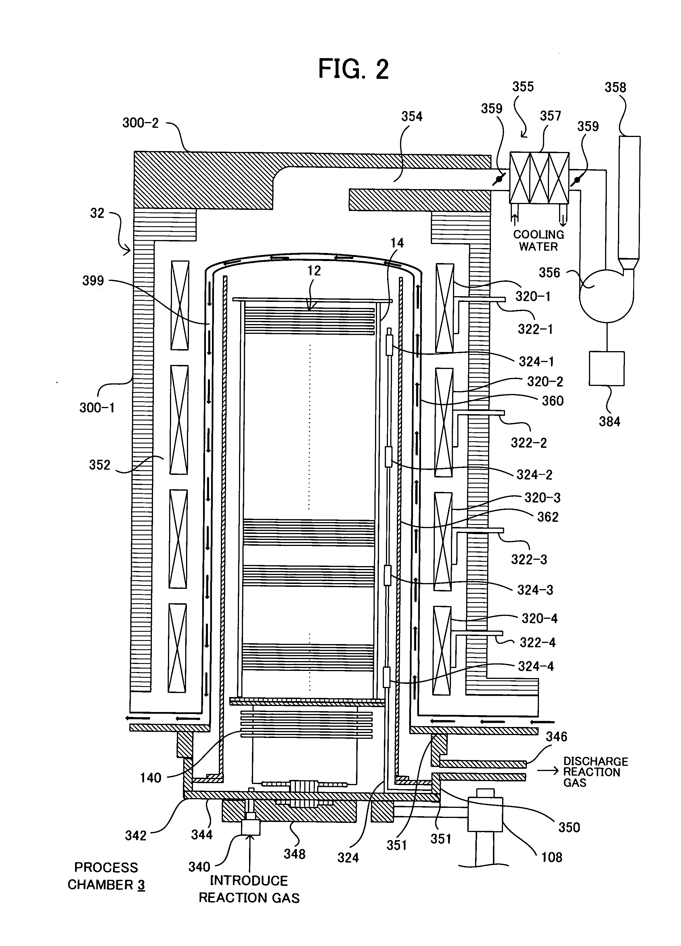
[0080]FIG. 2 is a view showing a process chamber 3 in a state where a boat 14 and wafers 12 shown in FIG. 1 are accommodated therein by way of example.

[0081]FIG. 3 is a view showing components on the periphery of the process chamber 3 shown in FIG. 1 and FIG. 2 and the configuration of a first control program 40 to control the process chamber 3.

[0082]The semiconductor processing apparatus 1 is a so-called low-pressure CVD apparatus that processes a substrate, for example, a semiconductor.

[0083]As is shown in FIG. 1, the semiconductor processing apparatus 1 is formed of a cassette exchanging unit 100, a cassette stoc...


PUM

PropertyMeasurementUnit
temperatureaaaaaaaaaa
flow rateaaaaaaaaaa
temperaturesaaaaaaaaaa

Abstract

A substrate processing apparatus has: a process chamber in which a substrate is processed; a heating device that optically heats the substrate accommodated in the process chamber from an outer periphery side of the substrate; a cooling device that cools the outer periphery side of the substrate by flowing a fluid in a vicinity of an outer periphery of the substrate optically heated by the heating device; a temperature detection portion that detects a temperature inside the process chamber; and a heating control portion that controls the heating device and the cooling device in such a manner so as to provide a temperature difference between a center portion of the substrate and an end portion of the substrate while maintaining a temperature at the center portion at a pre-determined temperature according to the temperature detected by the temperature detection portion.

Description

TECHNICAL FIELD[0001]The present invention relates to a substrate processing apparatus and a substrate processing method for processing a substrate, such as a semiconductor wafer.BACKGROUND ART[0002]For example, Patent Document 1 discloses a substrate processing apparatus that makes the thickness of a film deposited on the substrate uniform by controlling a heating temperature of the substrate by finding a variance temperature amount N to achieve a desired average temperature deviation M using a deviation between the temperature at the end portion and the temperature at the center portion of the substrate generated when the heating temperature of the substrate is varied within a predetermined time and a steady-state deviation between the temperature at the end portion and the temperature at the center portion of the substrate.[0003]However, even when the desired average temperature deviation M is achieved, there is a limit of uniformity for the thickness of a film deposited on the s...

Claims


Application Information

Patent Timeline
Patent Type & Authority Applications(United States)
IPC IPC(8): H01L21/66B05C11/00
CPCC23C16/46H01L21/67248H01L21/67109H01L21/324H01L21/02
Inventor UENO, MASAAKISHIMADA, MASAKAZUHANASHIMA, TAKEOMORIKAWA, HARUOHAYASHIDA, AKIRA
Owner KOKUSA ELECTRIC CO LTD
Why Eureka
Try Eureka