
Active matrix display apparatus and driving method thereof

a technology of active matrix and display apparatus, which is applied in the direction of instruments, static indicating devices, etc., can solve the problems of significant influence, insufficient current writing operation, and inability to write pixel circuit current, so as to improve current writing operation ability (prg ability), low drive current, and low luminance

Inactive Publication Date: 2009-02-05
CANON KK
View PDF16 Cites 23 Cited by
  • Summary
  • Abstract
  • Description
  • Claims
  • Application Information

AI Technical Summary

Benefits of technology

[0022]It is an aspect of the invention to solve such problem and improve current writing operation ability (PRG ability) in a low drive current (low luminance) region by simple means.
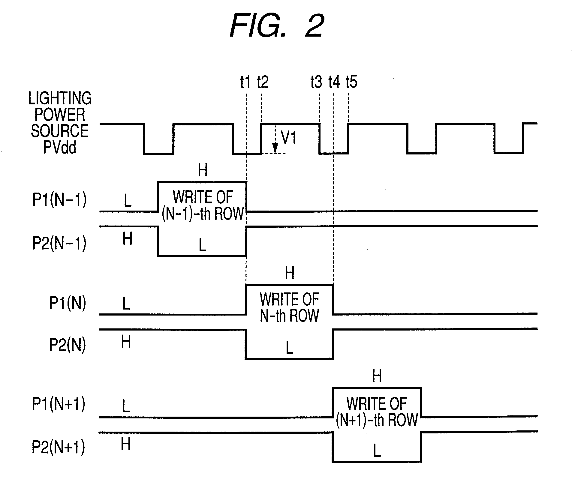
[0027]According to another aspect of the invention, a driving method of the active matrix type display apparatus including two-dimensionally arranged pixel circuits; and a plurality of signal lines and a plurality of scanning lines connected to the pixel circuits, each of the pixel circuit including a drive transistor and a capacitor a terminal of the capacitor is connected to a control terminal of said drive transistor, and the other terminal of said capacitor is connected to a first main conductive terminal of said drive transistor and a lighting power source, said driving method comprising the steps of: conducting the current flowing in said signal line into said drive transistor at the time of the writing operation; changing a potential of the lighting power source toward a potential of the signal line and keeping the changed potential for a period; injecting a current conducting said drive transistor into said display element at the time of the lighting operation, and recovering the potential of the lighting power source.
[0028]According to the present invention, the current writing operation ability (PRG ability) can be improved in a low drive current (low luminance) region with simple means.

Problems solved by technology

However, the current writing operation of the pixel circuit shown in FIGS. 5 and 6 is significantly affected by the parasitic capacitance value.
When the “PRG ability” value is not secured, the current writing operation becomes insufficient, and the display image quality is remarkably damaged.
The signal line parasitic capacitance is almost decided by the number of display rows and the display size, but the drastic reduction beyond the same is difficult.
However, when the current is set large, this causes a problem that deterioration of the brightness of the EL element is accelerated.

Method used


Image

  • Active matrix display apparatus and driving method thereof
  • Active matrix display apparatus and driving method thereof
  • Active matrix display apparatus and driving method thereof

Examples


Embodiment Construction

[0040]Exemplary embodiments of the present invention will be described below with reference to the drawings.

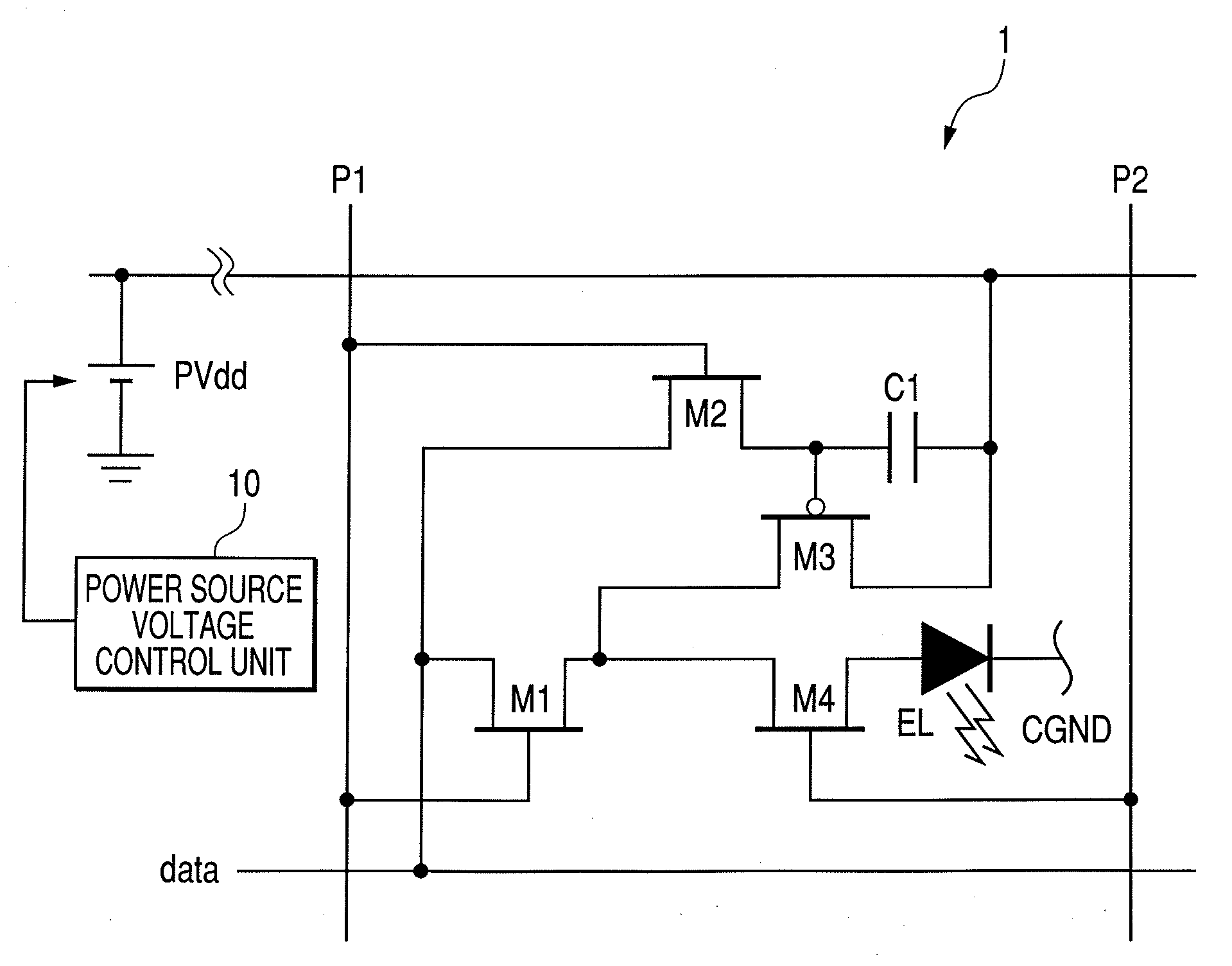
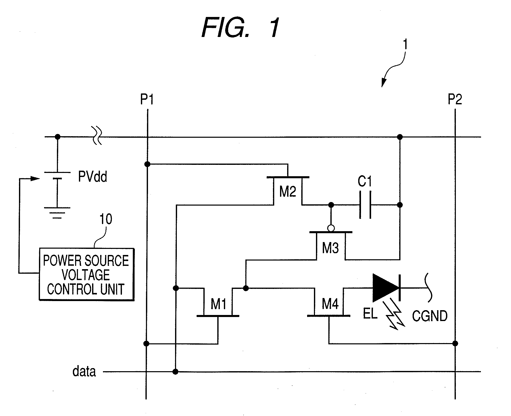
[0041]An EL panel (active matrix type display apparatus) according to the present embodiment uses a current writing type pixel circuit 1 shown in FIG. 1.

[0042]The pixel circuit 1 shown in FIG. 1 includes an EL element being a display element (referred to also as “OLED: Organic Light Emitting Diode”) and a drive circuit of the EL element. The drive circuit includes switch transistors (hereinafter, referred to as transistor) M1, M2, and M4 each including an n-type TFT, a transistor M3 including a p-type TFT, and a capacitor (capacitor or storage capacitor) C1. The pixel circuit 1 is connected with a light emission power source line PVdd, a ground line CGND, a signal line (data) for supplying a current Idata, two scanning lines P1 and P2 for supplying scanning signals to control an on-off operation of transistors M1, M2, and M4.

[0043]The EL element has an anode terminal (current ...


PUM


Abstract

An active matrix display apparatus comprising two-dimensional arranged pixel circuits each including a display element connected with a signal line for supplying a current thereto and a scanning line, and further including a drive transistor and a capacitor, one terminal thereof being connected to a control terminal of the drive transistor, wherein a first main conductive terminal of the drive transistor and the other terminal of the capacitor are connected to a lighting power source for supplying a current to the display element, and wherein at the current writing operation, the current supplied to the signal line is conducted to the drive transistor and at the lighting operation, the conductive current is injected into the display element so that before completion of the write operation, a voltage drop by a predetermined value is started to the voltage of the lighting power source and is kept continued for a predetermined period.

Description

BACKGROUND OF THE INVENTION[0001]1. Field of the Invention[0002]The present invention relates to an active matrix display apparatus using an electro-luminescence element (hereinafter, referred to as EL element) which emits light by injecting a current for an image display, and a driving method of the same. Hereinafter, in the present specification, the active matrix display apparatus using the EL element is referred to as an EL panel.[0003]2. Description of the Related Art[0004]Active Matrix Display Apparatus[0005]FIG. 4 illustrates an overall configuration example of a color EL panel. The color EL panel shown in the figure includes a column control circuit 3, a column register 5, a row register 6, and a control circuit 9 in addition to a display region 2 in which a pixel circuit 1 including a display element (EL element) and its drive circuit is two-dimensionally arranged.[0006]In the display region 2, a plurality of pixel circuits 1 is arranged in a matrix pattern along a row dire...

Claims


Application Information

Patent Timeline
IPC IPC(8): G09G3/30
CPCG09G3/3233G09G2320/043G09G2300/0819
Inventor KAWASAKI, SOMEIKAWANO, FUJIO
Owner CANON KK
Learn More