
Image processing apparatus and method

a technology of image processing and apparatus, applied in the field of image processing apparatus and method, can solve the problem that the technique of image processing speed is not sufficiently increased, and achieve the effect of reducing the size of circuitry and increasing the speed of image processing

Active Publication Date: 2009-02-05
CANON KK
View PDF26 Cites 14 Cited by
  • Summary
  • Abstract
  • Description
  • Claims
  • Application Information

AI Technical Summary

Benefits of technology

[0013]Objects of the present invention are to reduce the size of circuitry for image processing and to increase the speed of the image processing.

Problems solved by technology

While the related art techniques specify that pixels are scanned one by one in the direction of height of band areas in local image processing and make mention of reducing the size of delay memories, the related art techniques did not sufficiently increase the speed of image processing.

Method used


Image

  • Image processing apparatus and method
  • Image processing apparatus and method
  • Image processing apparatus and method

Examples


first embodiment

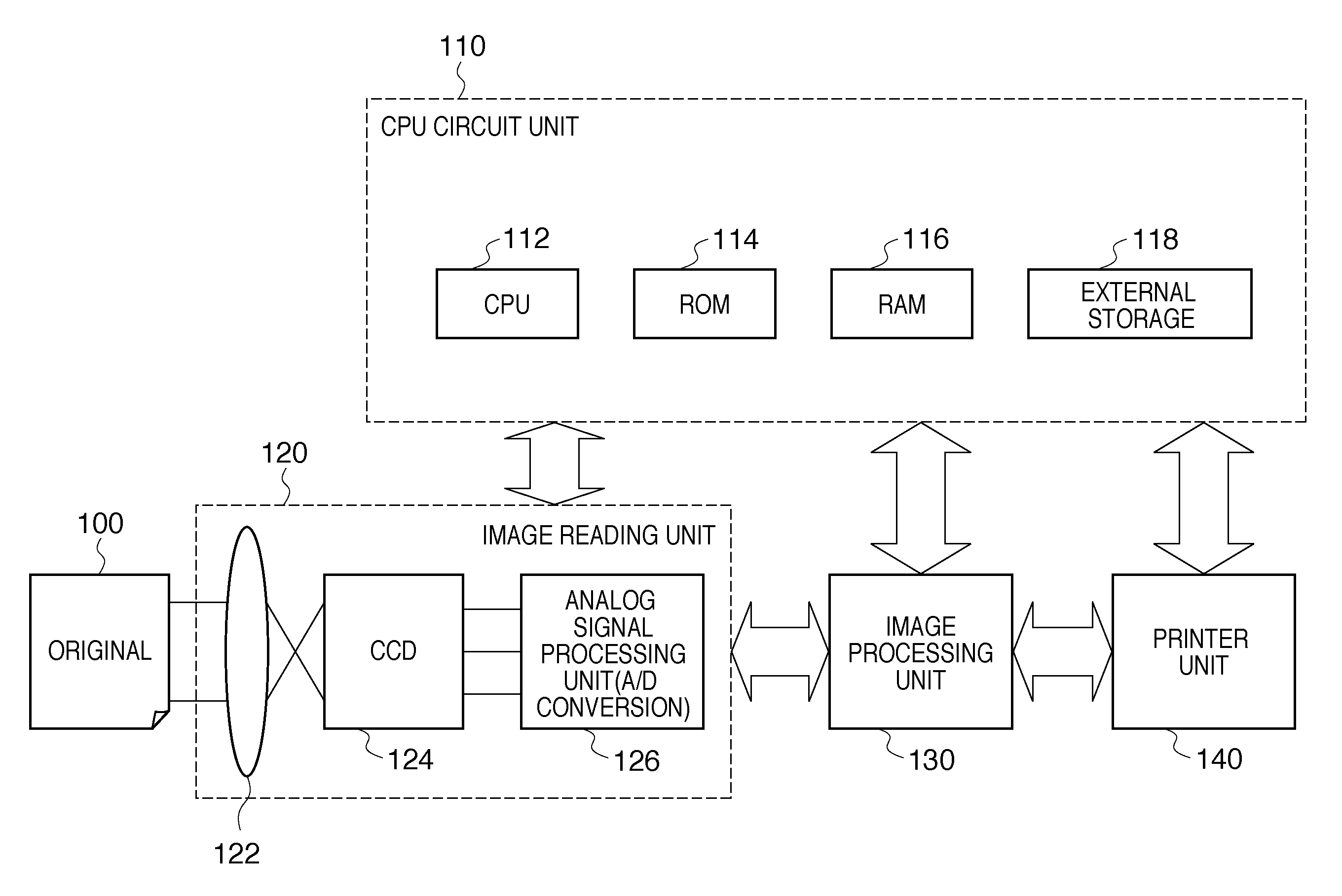
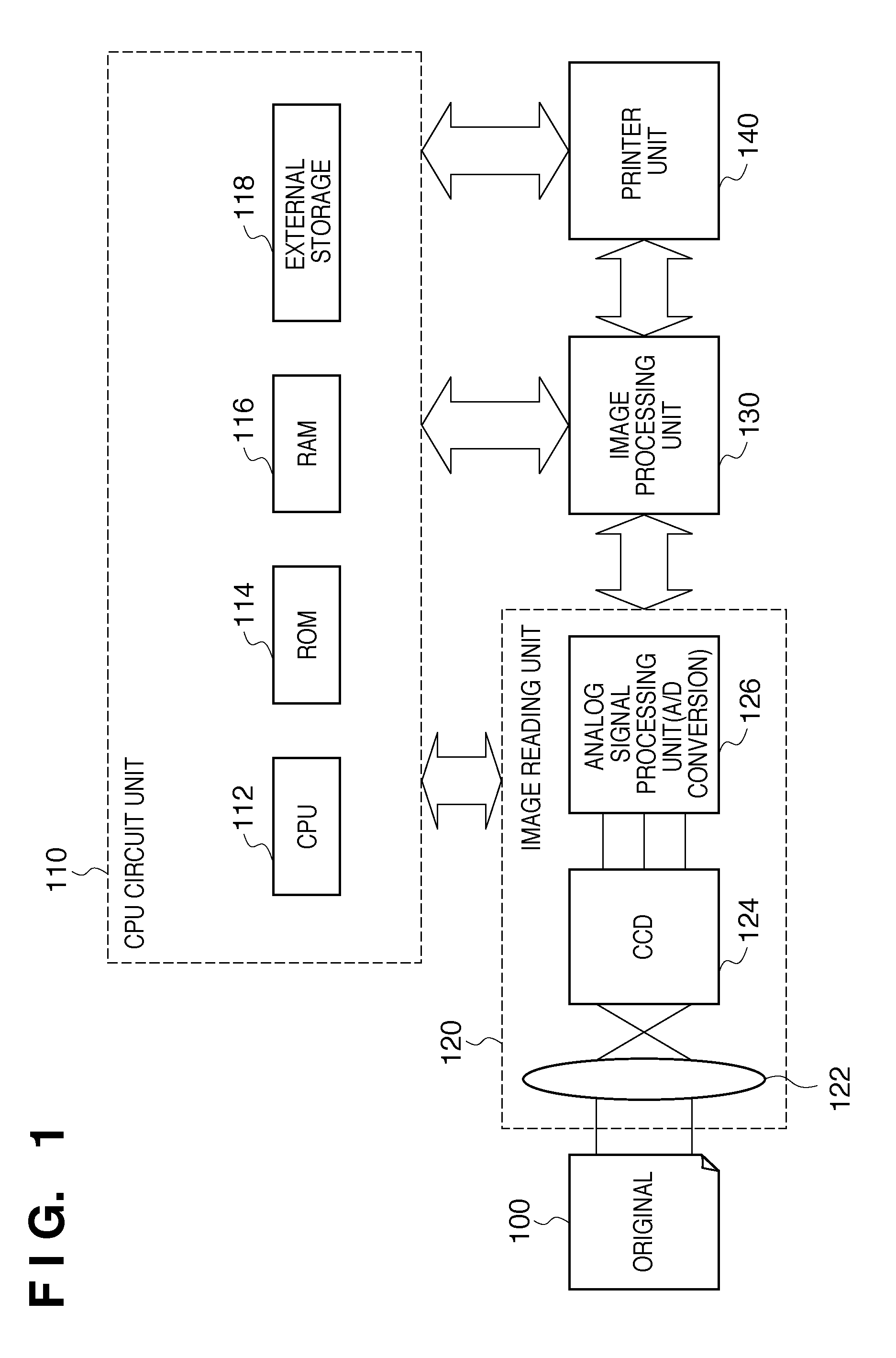
[0027]FIG. 1 is a block diagram showing an exemplary general configuration of an image processing apparatus according to a first embodiment. An image reading unit 120 in FIG. 1 includes a lens 122, a CCD sensor 124, and an analog signal processing unit 126. In the image reading unit 120, image information on an original 100 that is formed on the CCD sensor 124 through the lens 122 is converted by the CCD sensor 124 to analog electrical signals of R (Red), G (Green), and B (Blue).

[0028]The analog electrical signals converted from the image information are input into the analog signal processing unit 126, where processing such as correction is applied to the R, G, and B signals separately, and then the resulting signals are converted to digital signals (A / D conversion). Thus, a digital full-color signals (hereinafter referred to as the digital image signals) is generated. The generated digital image signals are input into an image processing unit 130. The image processing unit 130 app...

second embodiment

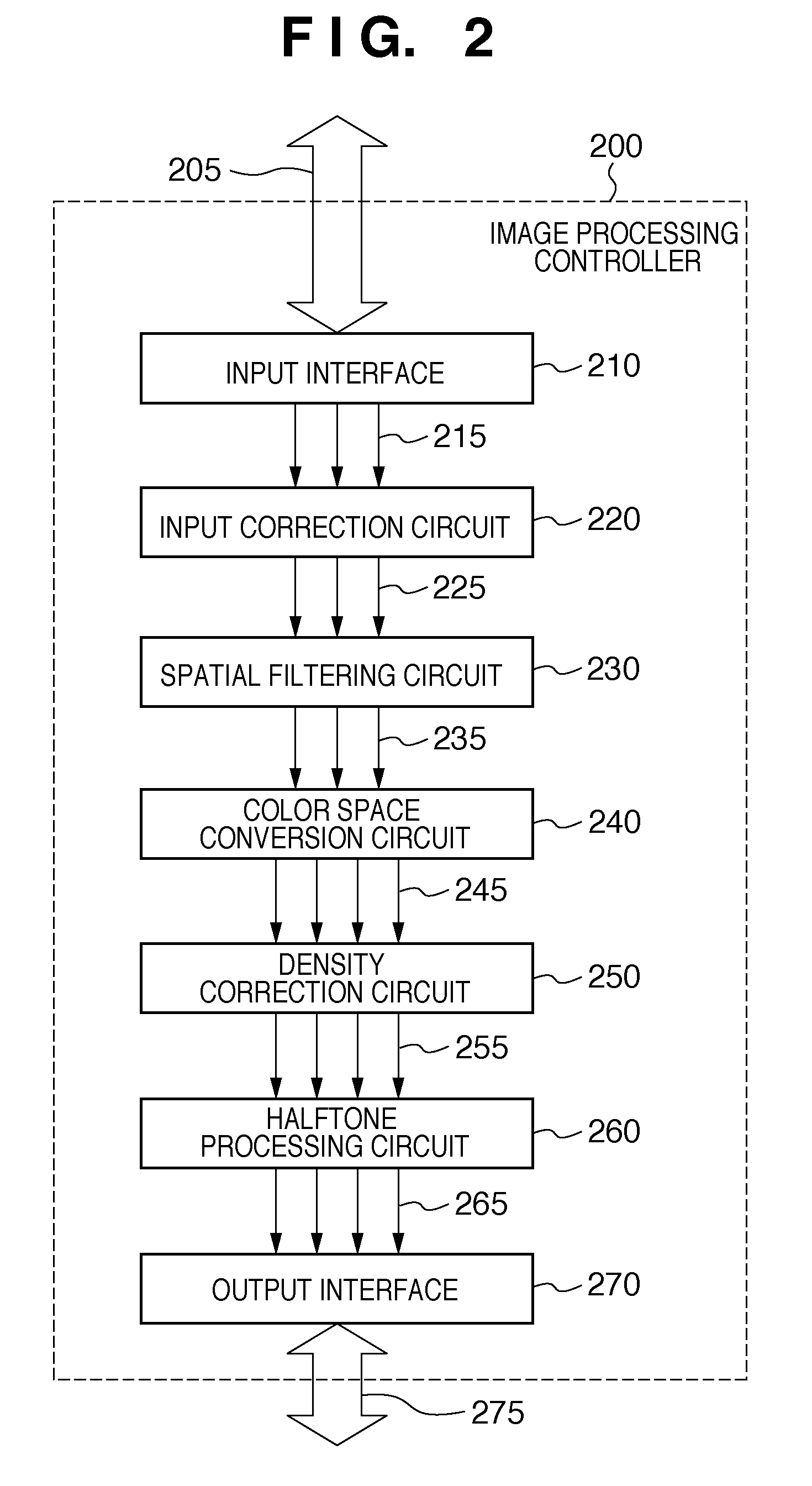
[0083]A second embodiment of the present invention will be described. In the second embodiment, N pixels in a pixel set are processed in a parallel distributed manner and therefore image processing faster than that in the first embodiment can be performed. By a method for increasing the speed of the processing described below, the speed of image processing can be increased in keeping with increase of the resolution of digital image data. In the description of the second embodiment, the same elements as those in the first embodiment described above are labeled with the same reference numerals or symbols as those in FIGS. 1 to 6A and 6B and further description thereof will be omitted.

[0084]FIG. 7 shows a pixel region corresponding to FIG. 4E, that is, a region of processing object pixels temporarily held in a spatial filtering circuit 230. As can be seen from FIG. 7, four patterns of spatial filters (nine pixels) 701 to 704 can be extracted at the same time for a set of four input pix...


PUM


Abstract

An image processing apparatus reads a unit of first image data corresponding to a first region, a unit of pixels at a time, from a first memory storing image data in a band area and reads second image data to be used in processing of multiple processing object pixels corresponding to the first region from a second memory. The image processing apparatus processes each of the multiple processing object pixels by using pixels in a second region containing each of the multiple processing object pixels and stores data of pixels contained in the first image data to be used in processing of other multiple pixels in the second memory.

Description

BACKGROUND OF THE INVENTION[0001]1. Field of the Invention[0002]The present invention relates to an image processing apparatus and method.[0003]2. Description of the Related Art[0004]Local (neighborhood) image processing such as spatial filtering has been performed when an image is generated and output. Local image processing is image processing in which some computation is performed using all pixels in a spatial filter area containing the pixels to be processed (hereinafter simply referred to as processing object pixels).[0005]For example, spatial filtering such as edge enhancement or blurring is applied to digital image data 300 shown in FIG. 3A. There are local image processing techniques in which digital image data is divided into areas and local image processing is performed in each of the areas (see U.S. Pat. No. 6,587,158, Japanese Patent Application Laid-Open No. 2000-312327, U.S. Pat. No. 6,950,559, and Japanese Patent Application Laid-Open No. 2006-139606). These technique...

Claims


Application Information

Patent Timeline
Patent Type & Authority Applications(United States)
IPC IPC(8): H04N5/956
CPCG06T1/60G06T5/20H04N5/91H04N5/772H04N5/765
Inventor ITO, TADAYUKI
Owner CANON KK
Learn More