Method and Apparatus for Providing Electrically Isolated Closely Spaced Features on a Printed Circuit Board

a technology of printed circuit board and closely spaced features, which is applied in the direction of programmable/customizable/modifiable circuits, electrical apparatus contruction details, and printed circuit non-printed electric components association. it can solve the problem of increasing surface roughness, limit of resolution between two metal conductors, and limited graphic arts technology

Inactive Publication Date: 2009-02-05
MOTOROLA SOLUTIONS INC
View PDF9 Cites 8 Cited by
  • Summary
  • Abstract
  • Description
  • Claims
  • Application Information

AI Technical Summary

Problems solved by technology

However, current graphic arts technology is limited in the feature size that can be achieved, the current limit of resolution between two metal conductors being about 10-50 micrometers.
Although these techniques can alter the substrat

Method used


Image

  • Method and Apparatus for Providing Electrically Isolated Closely Spaced Features on a Printed Circuit Board
  • Method and Apparatus for Providing Electrically Isolated Closely Spaced Features on a Printed Circuit Board
  • Method and Apparatus for Providing Electrically Isolated Closely Spaced Features on a Printed Circuit Board

Examples


Embodiment Construction

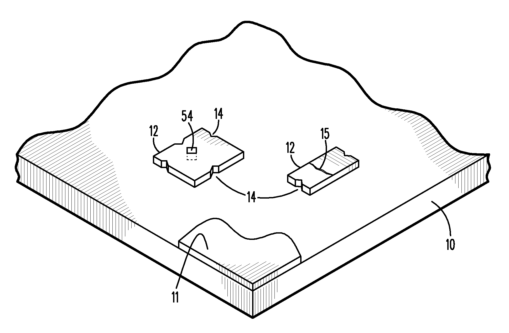
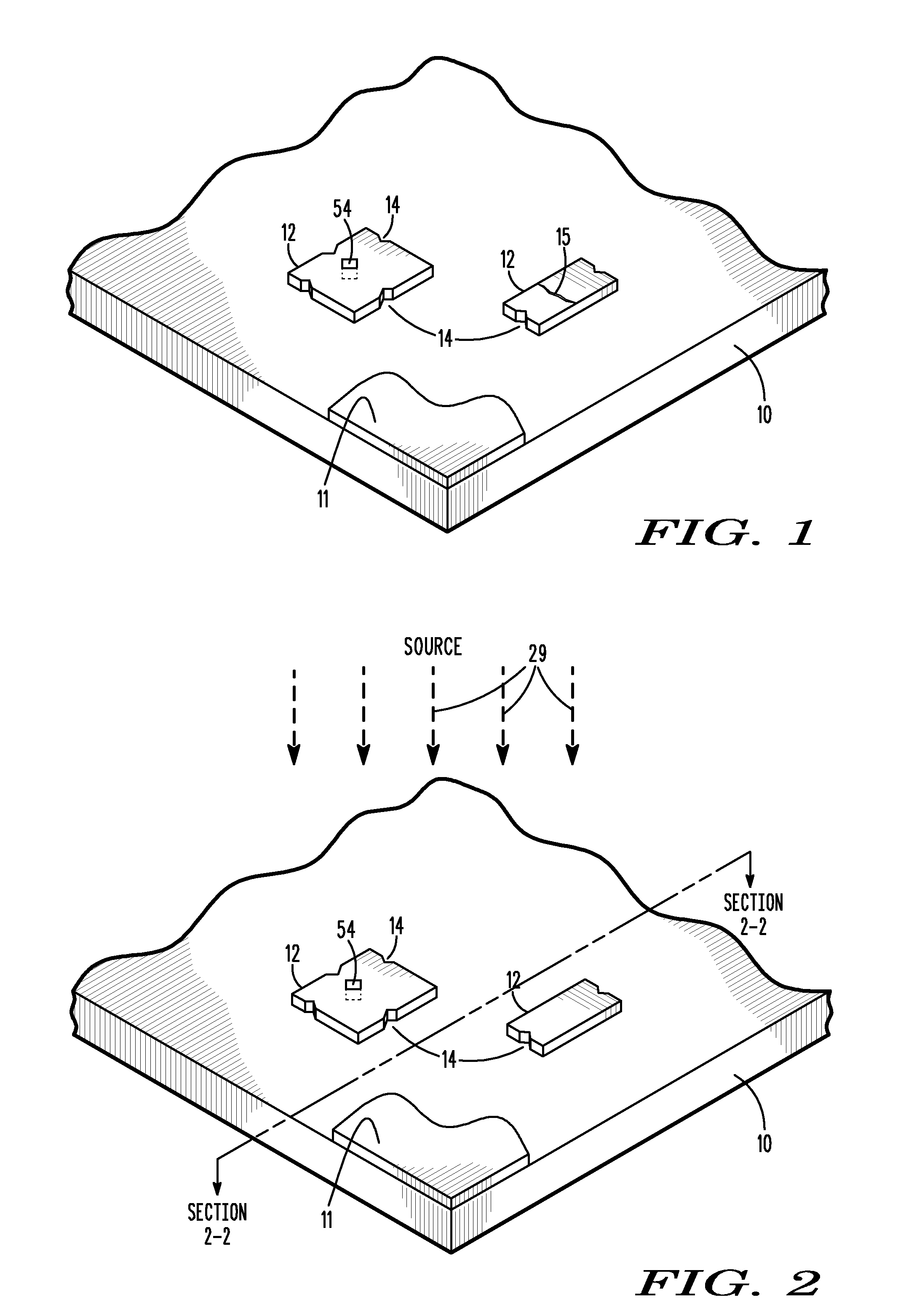
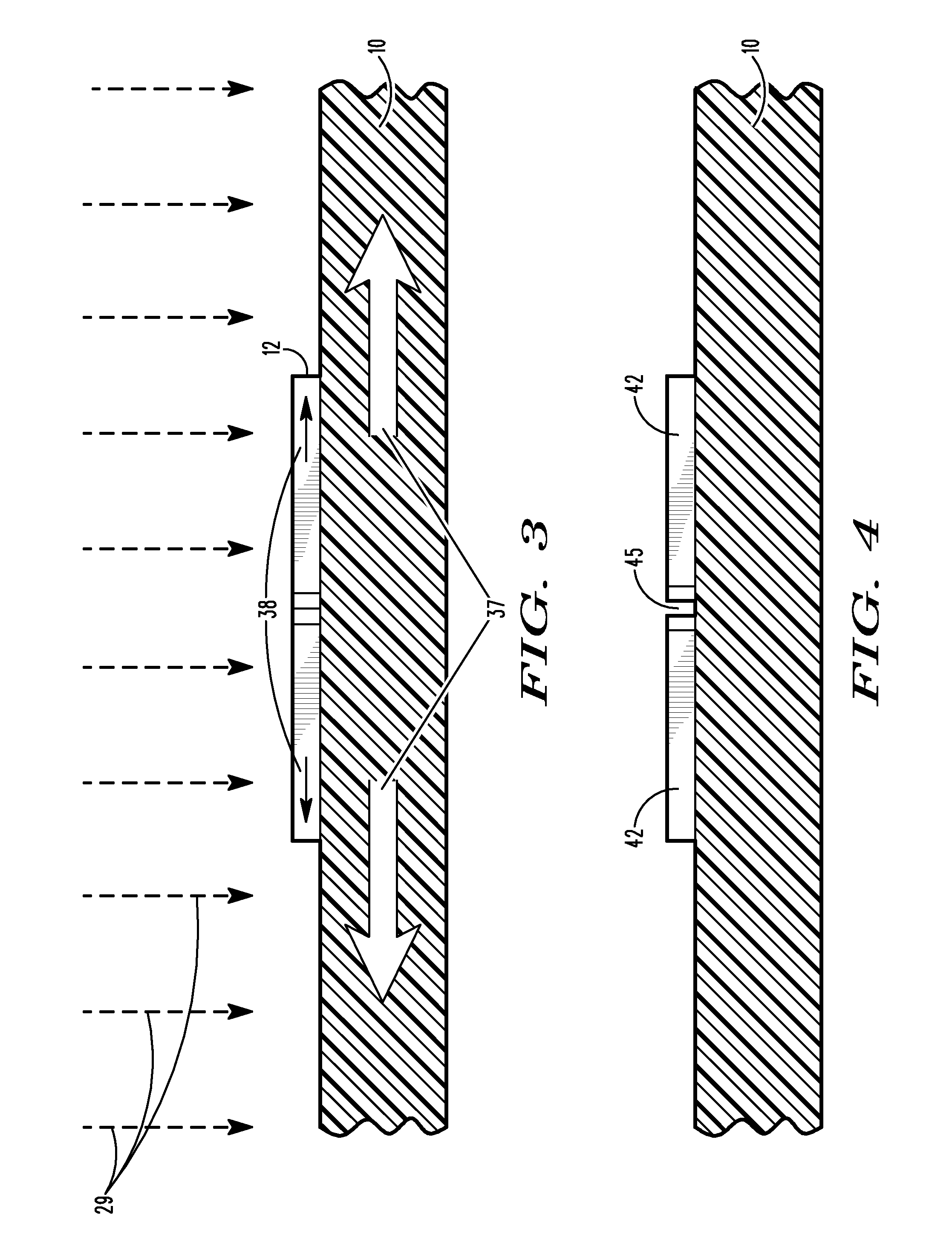
[0011]Before describing in detail embodiments that are in accordance with the present invention, it should be observed that the embodiments reside primarily in combinations of method and apparatus components related to a method and apparatus for providing electrically isolated closely spaced features on a printed circuit board. Accordingly, the apparatus components and methods have been represented where appropriate by conventional symbols in the drawings, showing only those specific details that are pertinent to understanding the embodiments of the present invention so as not to obscure the disclosure with details that will be readily apparent to those of ordinary skill in the art having the benefit of the description herein.

[0012]In this document, relational terms such as first and second, top and bottom, and the like may be used solely to distinguish one entity or action from another entity or action without necessarily requiring or implying any actual such relationship or order ...


PUM

PropertyMeasurementUnit
Stress optical coefficientaaaaaaaaaa
Perimeteraaaaaaaaaa
Thermal stressaaaaaaaaaa

Abstract

A method and apparatus for forming controlled stress fractures in metal produces electrically isolated, closely spaced circuit sub-entities for use on a metallized printed wiring board. A polymeric substrate has a layer of metal adhered to the surface, and the metal layer is formed into entities. Each entity has a fracture initiating feature formed into it, which serves to initiate and/or direct a stress crack that is induced in the metal. The entities are fractured in a controlled manner by subjecting the substrate and the entities to mechanical stress by a rapid thermal excursion, creating a stress fracture in the entity extending from the fracture initiating feature. The stress fracture divides each entity into two or more sub-entities that are electrically isolated from each other by the stress fracture. The resulting structure can be used to form circuitry requiring very fine spaces for high density printed circuit boards. The rapid thermal stress may be induced by a high intensity, strobed xenon arc lamp.

Description

FIELD OF THE INVENTION[0001]The present invention relates generally to fine features in metal circuitry on printed circuit boards, and more particularly, to a method for creating fine features using thermal and mechanical stressing.BACKGROUND[0002]Conventional fabrication methods for printed circuits have always utilized one or more methods of creating a conductive metal pattern on a dielectric substrate. Some of the various methods include print and etch, electroless copper deposition, vacuum deposition, and on-contact screen printing, contact printing, or ink jetting a liquid slurry of metal onto the substrate. Some of these methods are subtractive, such as the “print and etch” technique where patterns are etched from a laminated copper foil, others are purely additive, such as screen or thick film printing where conductor patterns are directly formed on the substrate, and still others are combinations of additive and subtractive. One technique that is gaining popularity is the fa...

Claims


Application Information

Patent Timeline
IPC IPC(8): H05K7/00H01R43/00
CPCH01L21/4846Y10T29/49117H01L23/49838H01L23/49866H01L29/78603H05K1/0293H05K3/04H05K3/22H05K2201/068H05K2201/09727H05K2203/1105H05K2203/1476H05K2203/175H01L2924/0002H01L23/145H01L2924/00
Inventor WIEGLUS, JERZYGAMOTA, DANIEL R.KLOSOWIAK, TOMASZ L.SZCZECH, JOHN B.TSUI, KIN P.
Owner MOTOROLA SOLUTIONS INC
Why Eureka
Try Eureka