High-voltage mos transistor device

a transistor device and high-voltage mos technology, applied in the direction of semiconductor devices, basic electric elements, electrical equipment, etc., can solve problems such as damage to hv mos transistor devices, and achieve the effect of smooth electrical field distribution

Active Publication Date: 2009-02-12
UNITED MICROELECTRONICS CORP
View PDF10 Cites 22 Cited by
  • Summary
  • Abstract
  • Description
  • Claims
  • Application Information

AI Technical Summary

Benefits of technology

[0009]In order to smooth the distribution of the electrical field, the HV MOS transistor device of the present invention has the first interface positioned

Problems solved by technology

This is greater than the breakdown voltage of most HV MOS transisto

Method used


Image

  • High-voltage mos transistor device
  • High-voltage mos transistor device
  • High-voltage mos transistor device

Examples


Embodiment Construction

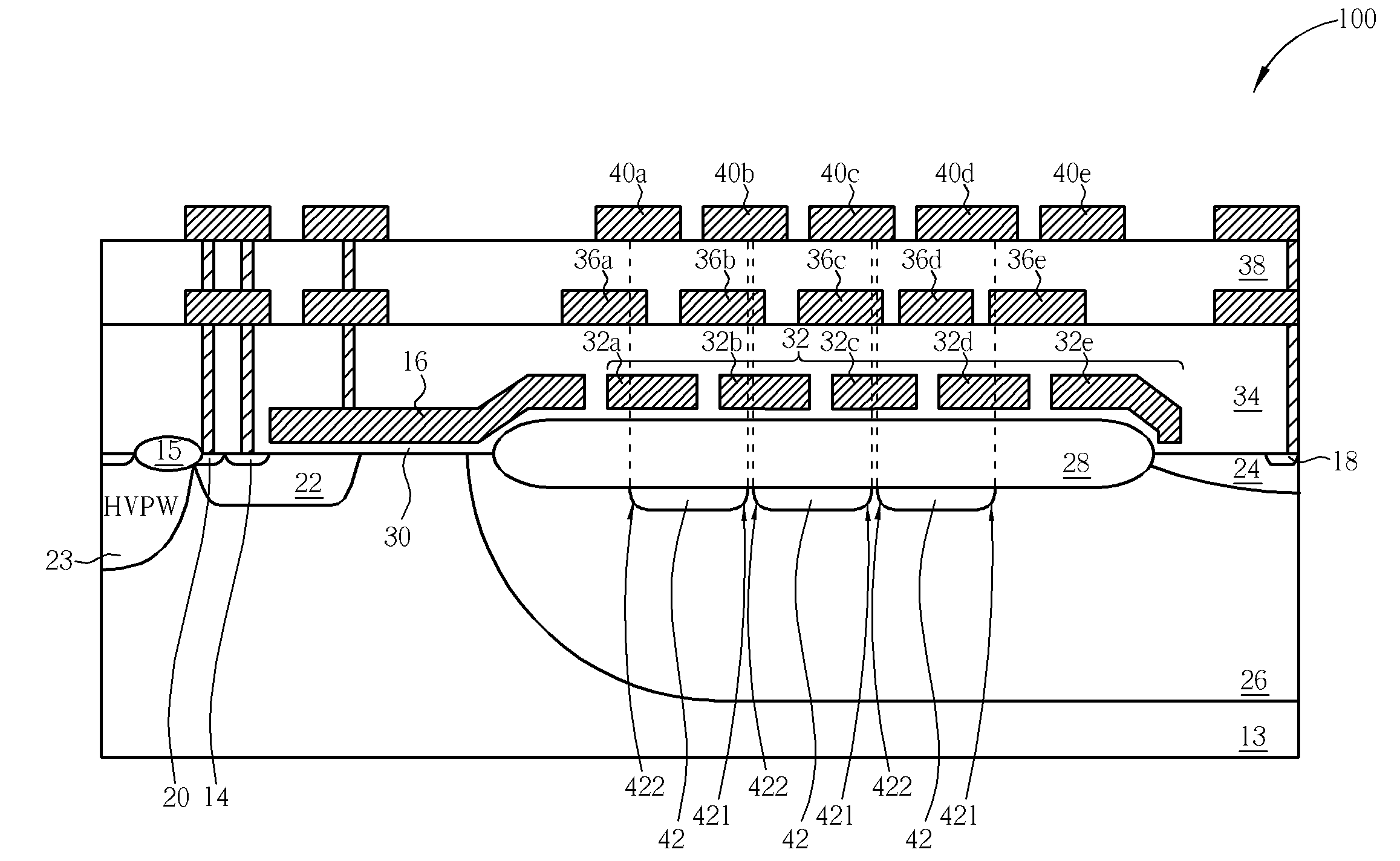
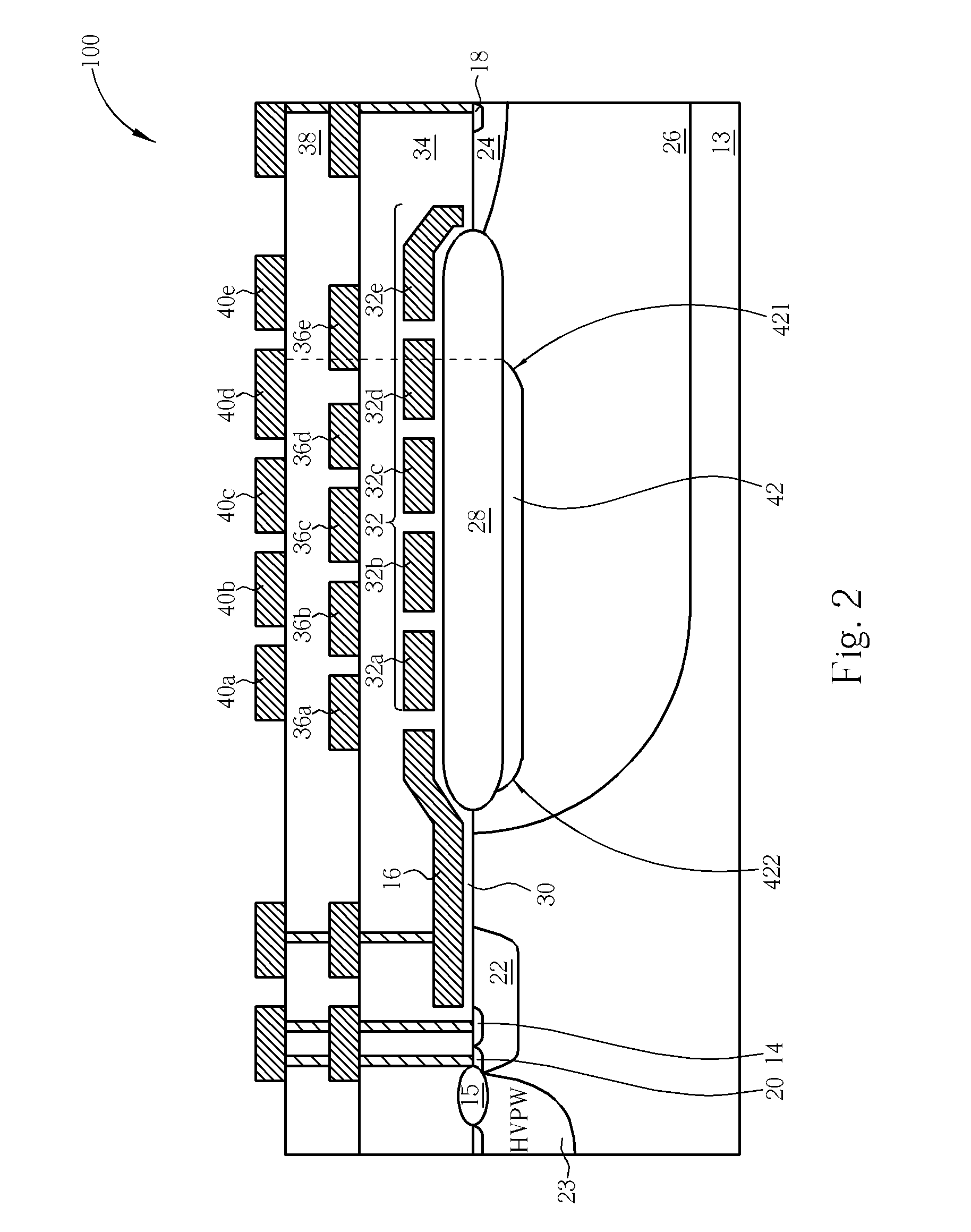
[0017]Hereinafter, preferred embodiments of the present invention will be described with reference to the accompanying drawings, in which components with substantially the same functions are identified by the same reference numeral for the sake of simplicity. The following description of the present invention will focus on a HV MOS transistor device with a high breakdown voltage of at least 700V. It should be noted, however, that the present invention is in no way limited to the following illustrative embodiments. While the following discussions are described below using P-channel devices, the discussion also pertains to N-channel devices, which may be formed by reversing the conductivity of the described regions and layers.

[0018]Please refer to FIG. 2, which shows a cross-section diagram of a HV MOS transistor device 100 according to a first preferred embodiment of the present invention. The HV MOS transistor device 100 is formed on a substrate 13, such as a P doped silicon substra...


PUM


Abstract

A HV MOS transistor device having a substrate, a gate, a source, a drain, a first ion well of a first conductive type disposed in the substrate, and a plurality of field plates disposed on the substrate is disclosed. The HV MOS transistor device further has a first doped region of a second conductive type positioned in the first ion well. Therefore, a first interface and a second interface between the first ion well and the first doped region are formed, and the first interface and the second interface are respectively positioned near the drain and the source. In addition, the first interface is positioned under a respective field plate to produce a smooth field distribution and to increase the breakdown voltage of the HV transistor device.

Description

BACKGROUND OF THE INVENTION[0001]1. Field of the Invention[0002]The present invention relates to a high-voltage MOS (HV MOS) transistor device, and particularly, to a HV MOS transistor device having a P doped region positioned in an N ion well and a plurality of field plates to produce a smooth field distribution when subject to a high drain voltage and prevent the HV MOS transistor device from breakdown.[0003]2. Description of the Prior Art[0004]Current power systems provide an alternating current having a variety of frequencies ranging from 50 to 60 Hz, and a voltage ranging from 100 to 240 volts (V). Every electrical device has a particular working voltage and frequency condition, and therefore, electrical devices and related passive elements utilized in the electrical devices, such as inductors, capacitors, resistors and transformers, act as a switch to determine the value of the voltage and the type of the current thereof. For example, a conventional air conditioner utilizes a ...

Claims


Application Information

Patent Timeline
IPC IPC(8): H01L29/78
CPCH01L29/0634H01L29/0878H01L29/7835H01L29/42368H01L29/404
Inventor SHU, SHIH-MINGHUANG, CHIH-JENCHENG, TUN-JENSU, CHAO-YUAN
Owner UNITED MICROELECTRONICS CORP
Why Eureka
Try Eureka