Thin film transistor and liquid crystal display having the same

a thin film transistor and liquid crystal display technology, applied in the direction of optics, semiconductor devices, instruments, etc., can solve the problems of reducing storage capacitance, difficult to drive the above-described lcd at a frame refresh rate, and the dot inversion driving method may not be available for high-resolution lcds such as full-hd (high definition) lcds, so as to achieve the effect of improving the aperture ratio

Active Publication Date: 2009-02-12
SHENZHEN CHINA STAR OPTOELECTRONICS TECH CO LTD
View PDF4 Cites 26 Cited by
  • Summary
  • Abstract
  • Description
  • Claims
  • Application Information

AI Technical Summary

Benefits of technology

[0013]Exemplary embodiments of the present invention provide a TFT substrate and an LCD having the same which may improve an aperture ratio by overlapping a pixel electrode and a data line.

Problems solved by technology

However, this may lead to a decrease in storage capacitance due to the thick low-dielectric-constant insulation layer provided between the storage electrode line and the pixel electrode even though the storage electrode line and the vertical part overlap each other.
Further, it may be difficult to drive the above-described LCD at a frame refresh rate of 120 Hz using a dot inversion driving method.
Therefore, the dot inversion driving method may not be available for high-resolution LCDs such as Full-HD (high definition) LCDs.
However, it may be very difficult to form a low-resistance interconnection, as the LCD becomes greater and requires higher resolution than ever before.
Consequently, as a result, this may produce vertical crosstalk, which in turn may lead to display defects.

Method used


Image

  • Thin film transistor and liquid crystal display having the same
  • Thin film transistor and liquid crystal display having the same
  • Thin film transistor and liquid crystal display having the same

Examples


Embodiment Construction

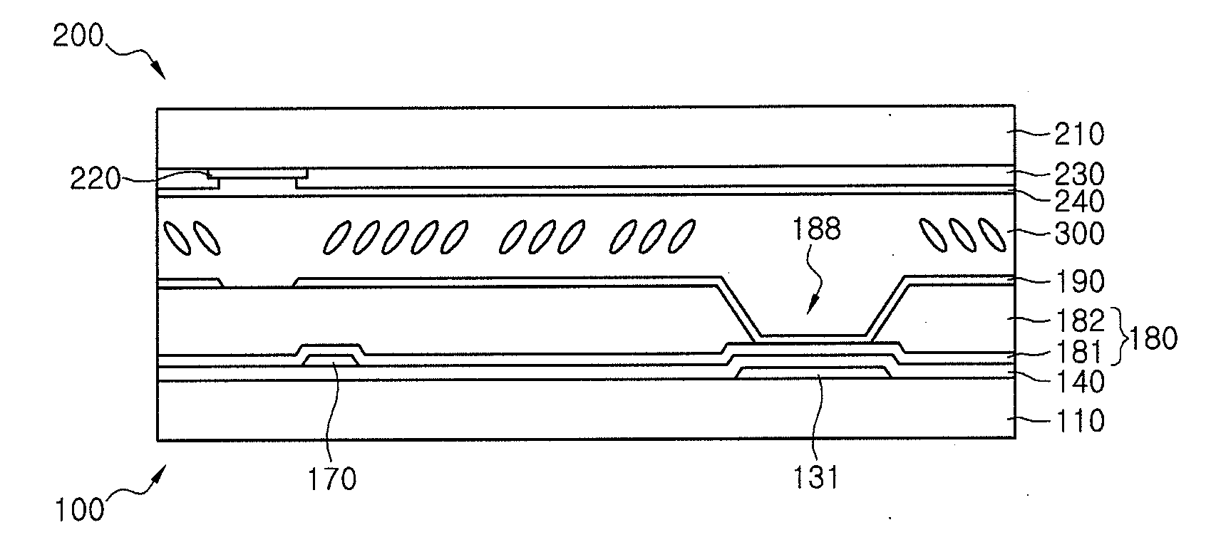
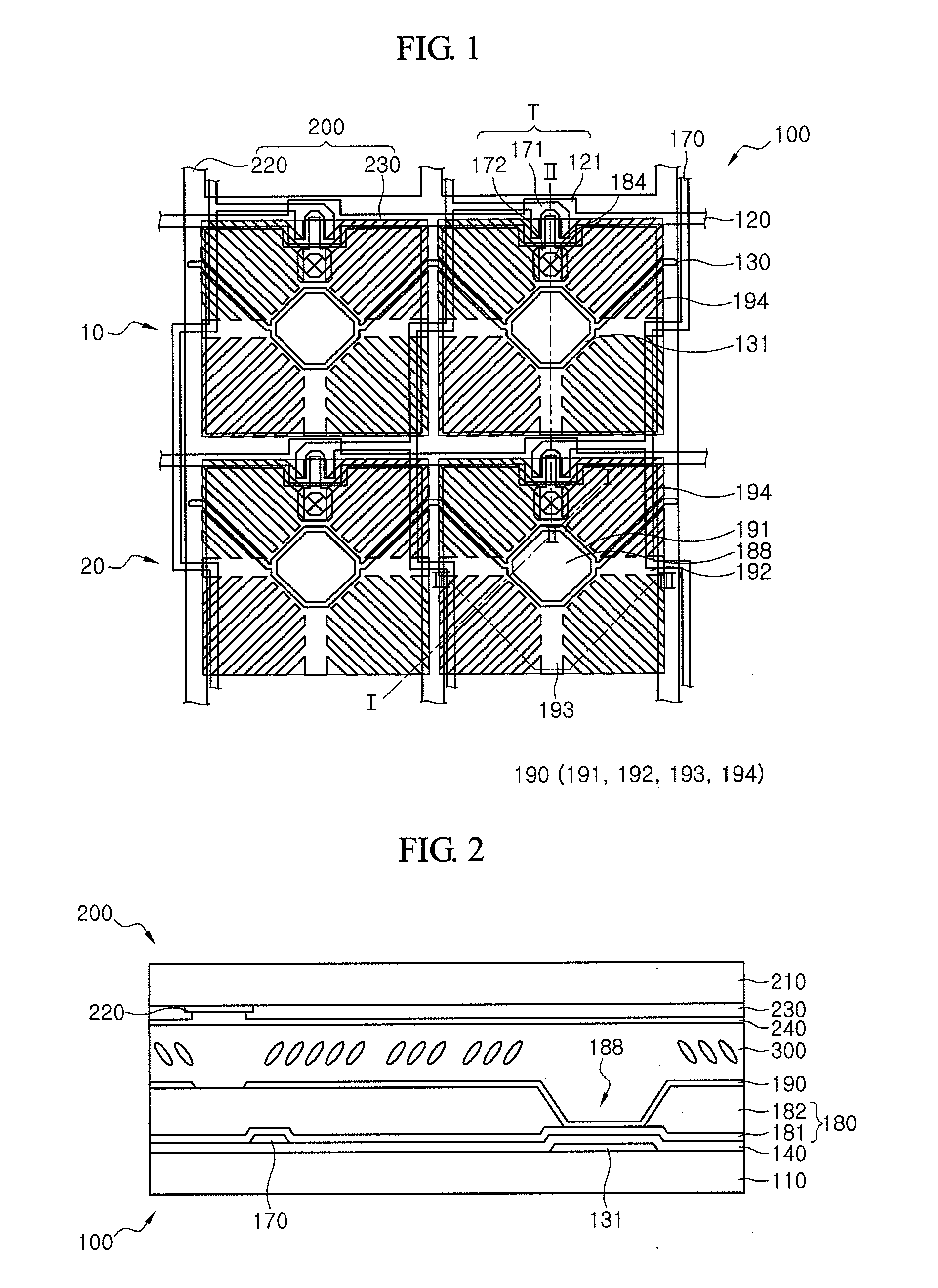
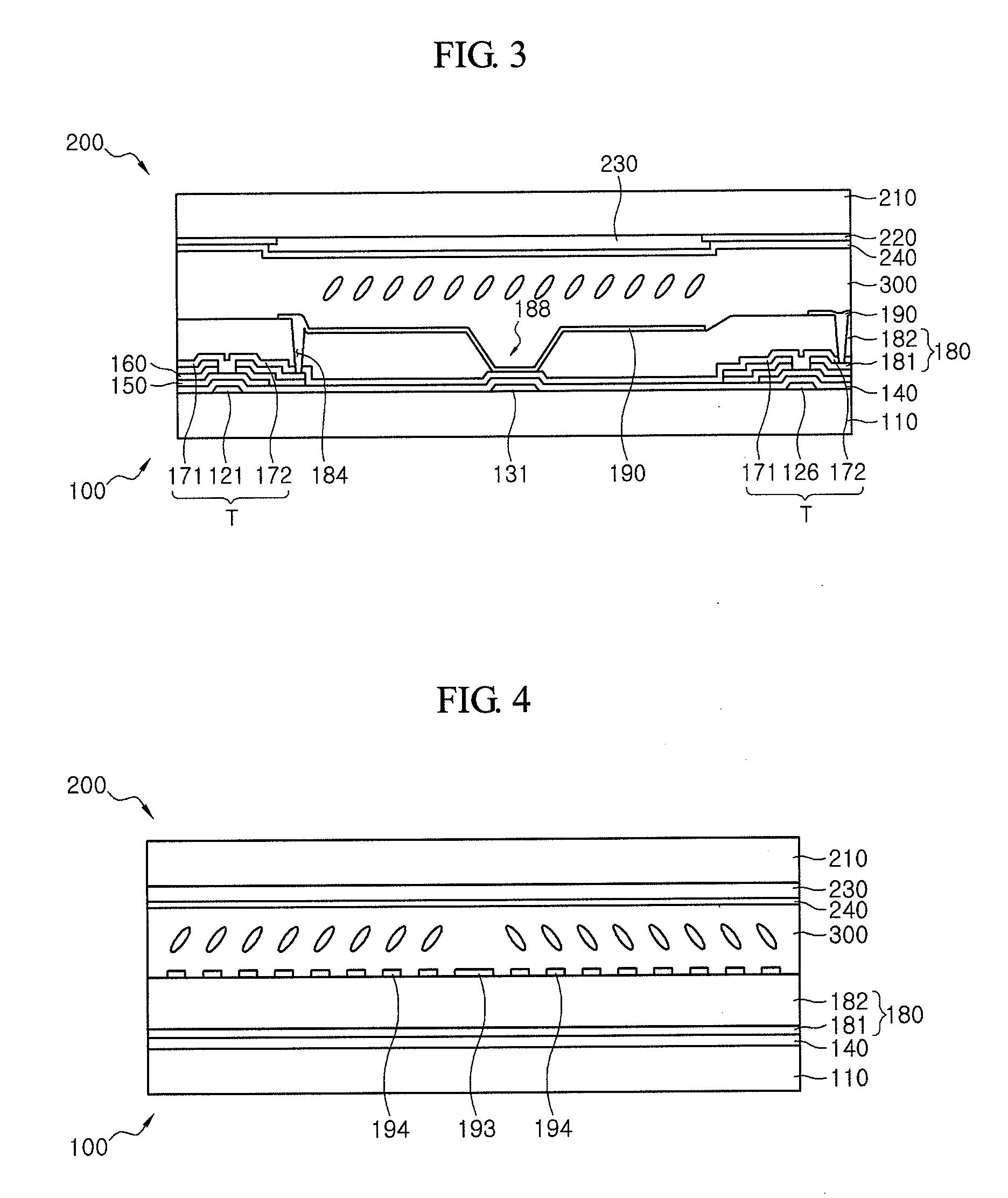
[0038]Hereinafter, specific embodiments will be described in detail with reference to the accompanying drawings. The present invention may, however, be embodied in different forms and should not be construed as being limited to the exemplary embodiments set forth herein. In the figures, the dimensions of layers and regions are exaggerated for clarity of illustration, and like reference numerals refer to like elements throughout. It will also be understood that when a layer (or film) is referred to as being ‘on’ another layer or substrate, it can be directly on the other layer or substrate, or intervening layers may also be present. Further, it will be understood that when a layer is referred to as being ‘under’ another layer, it can be directly under, and one or more intervening layers may also be present. In addition, it will also be understood that when a layer is referred to as being ‘between’ two layers, it can be the only layer between the two layers, or one or more intervening...


PUM

PropertyMeasurementUnit
electric fieldaaaaaaaaaa
tilting anglesaaaaaaaaaa
wide viewing angleaaaaaaaaaa

Abstract

A thin film transistor (TFT) substrate includes: a plurality of gate lines extending in one direction, a plurality of data lines extending in a direction intersecting the gate lines, a pixel electrode formed in a pixel region defined by an intersection of the gate line and the data line, and with one side of the pixel electrode overlapping a portion of one data line and another side of the pixel electrode overlapping a portion of another data line. The TFT further includes a storage electrode line having a storage electrode disposed in a central portion of the pixel region.

Description

CROSS-REFERENCE TO RELATED APPLICATION[0001]This application claims priority to Korean Patent Application No. 10-2007-0079405 filed on Aug. 8, 2007, the disclosure of which is hereby incorporated by reference in its entirety.BACKGROUND OF THE INVENTION[0002]1. Technical Field[0003]The present disclosure relates to a thin film transistor substrate and a liquid crystal display having the same.[0004]2. Description of the Related Art[0005]Liquid crystal displays (“LCD”s) typically include lower and upper substrates having field-generating electrodes, e.g., a pixel electrode and a common electrode, respectively, and a liquid crystal layer interposed between the lower and upper substrates. LCDs display an image in such a way that orientations of liquid crystal molecules in the liquid crystal layer are determined by applying a voltage to the field generating electrodes to generate an electric field across the liquid crystal layer and polarization of incident light is controlled.[0006]Among...

Claims


Application Information

Patent Timeline
Patent Type & Authority Applications(United States)
IPC IPC(8): G02F1/136H01L29/04
CPCG02F1/136213G02F1/136286H01L27/124H01L27/13G02F2001/134345G02F1/134345G02F1/136G02F1/1343
Inventor KIM, DONG GYU
Owner SHENZHEN CHINA STAR OPTOELECTRONICS TECH CO LTD
Why Eureka
Try Eureka