

Lithographic apparatus and device manufacturing method
- Summary
- Abstract
- Description
- Claims
- Application Information
AI Technical Summary
Benefits of technology
Problems solved by technology
Method used
Image


Examples
Embodiment Construction
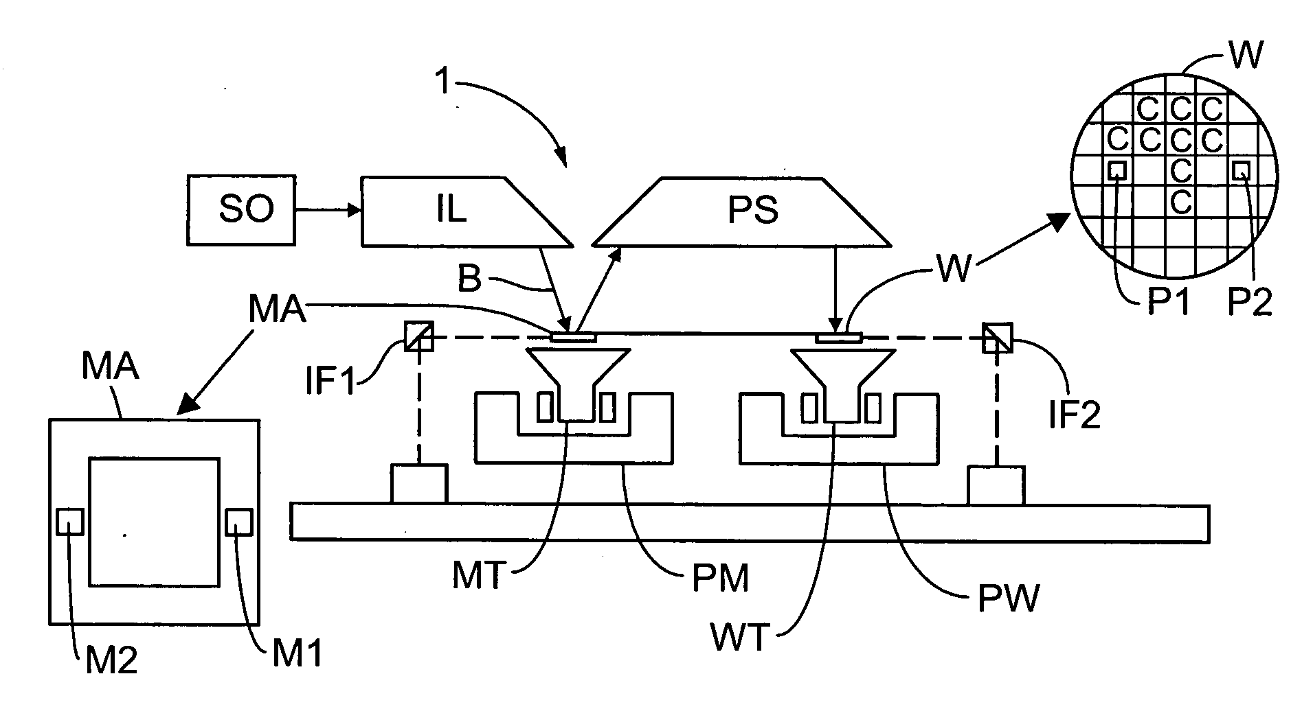
[0020]FIG. 1 schematically depicts a lithographic apparatus 1 according to an embodiment of the present invention. The apparatus 1 includes a source SO configured to generate radiation, an illumination system (illuminator) IL configured to condition a radiation beam B (e.g. EUV radiation) from the radiation received from source SO. The source SO may be provided as a separate unit. A support or pattern support (e.g. a mask table) MT is configured to support a patterning device (e.g. a mask) MA and is connected to a first positioning device PM configured to accurately position the patterning device MA in accordance with certain parameters. A substrate table or substrate support (e.g. a wafer table) WT is configured to hold a substrate (e.g. a resist-coated wafer) W and is connected to a second positioning device PW configured to accurately position the substrate W in accordance with certain parameters. A projection system (e.g. a refractive projection lens system) PS is configured to ...
PUM
 Abstract
Description
Claims
Application Information