Method for driving multi-level data to a phase change memory device
- Summary
- Abstract
- Description
- Claims
- Application Information
AI Technical Summary
Benefits of technology
Problems solved by technology
Method used
Image
Examples
Embodiment Construction
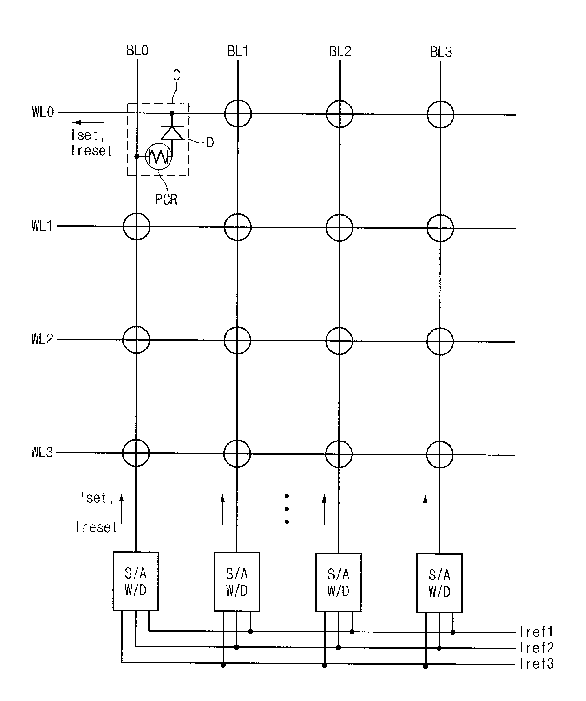
[0035]FIG. 4 is a diagram showing a phase change memory device according to an embodiment of the present invention.
[0036]The phase change memory device includes a plurality of bit lines BL0˜BL3 arranged in a row direction and a plurality of word lines WL0˜WL3 arranged in a column direction. A unit cell C is arranged at an intersection of the bit lines BL0˜BL3 the word lines WL0˜WL3. The unit cell C includes a phase change resistor PCR and a diode D. The diode D includes a PN diode element.
[0037]The phase change resistor PCR has one electrode connected to the bit line BL and the other electrode connected to a P-type region of the diode D. A N-type region of the diode D is connected to the word line WL.
[0038]A low voltage is applied to a selected word line WL in a read mode. A read voltage Vread is applied to the bit line BL so that a read current Iset having a set state and a read current Ireset having a reset state, flow toward the word line WL through the bit line BL, the phase cha...
PUM
 Abstract
Description
Claims
Application Information


