Non-volatile memory device including charge trap layer and method of manufacturing the same

a non-volatile memory and charge trap technology, which is applied in the direction of semiconductor devices, basic electric elements, electrical appliances, etc., can solve the problems of unreliability of the charge-trap memory device operation and the decrease of the operating speed of the charge-trap memory device, so as to reduce the operating speed, the effect of charging leakage and extending the band tail

Inactive Publication Date: 2009-02-26
SAMSUNG ELECTRONICS CO LTD
View PDF2 Cites 3 Cited by
  • Summary
  • Abstract
  • Description
  • Claims
  • Application Information

AI Technical Summary

Benefits of technology

[0026]According to the non-volatile material device of the present invention, a charge trap layer has a crystalline structure so that charge carriers can be trapped at a specific ...

Problems solved by technology

When an amorphous silicon nitride layer is used as a charge trap layer of a charge-trap memory device, the charge-trap memory device can operate unreliably due to an extended band tail of the amorphous silicon nitride.
Furthermore, the operating speed of the charge-trap memory devic...

Method used


Image

  • Non-volatile memory device including charge trap layer and method of manufacturing the same
  • Non-volatile memory device including charge trap layer and method of manufacturing the same
  • Non-volatile memory device including charge trap layer and method of manufacturing the same

Examples


Embodiment Construction

[0035]A non-volatile memory device and a method of manufacturing the non-volatile memory device will now be described more fully with reference to the accompanying drawings, in which exemplary embodiments of the invention are shown.

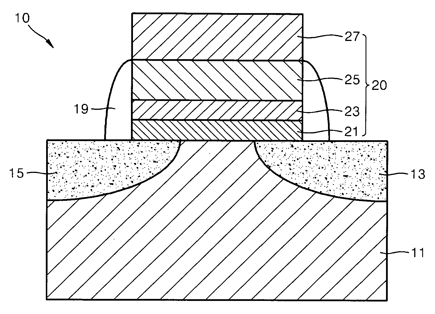
[0036]FIG. 1 is a schematic view illustrating a non-volatile memory device 10 according to an embodiment of the present invention. The non-volatile memory device 10 includes a substrate 11 and a gate structure 20 formed on the substrate 11. The substrate 11 may include first and second impurity regions 13 and 15 doped with a predetermined conductive impurity. For example, the first and second impurity regions 13 and 15 can be N+ doped regions. One of the first and second impurity regions 13 and 15 can be used as a drain (D), and the other can be used as a source (S).

[0037]The gate structure 20 includes a tunneling insulating layer 21 formed on the substrate 11, a charge trap layer 23 formed on the tunneling insulating layer 21, and a blocking insulating l...


PUM


Abstract

Provided are a non-volatile memory device and a method of manufacturing the non-volatile memory device. The non-volatile memory device includes a charge trap layer having a crystalline material. In the method, a tunneling insulating layer is formed on a substrate, and a crystalline charge trap layer is formed on the tunneling insulating layer.

Description

CROSS-REFERENCE TO RELATED PATENT APPLICATION[0001]This application claims the benefit of Korean Patent Application No. 10-2007-0084600, filed on Aug. 22, 2007, in the Korean Intellectual Property Office, the disclosure of which is incorporated herein in its entirety by reference.BACKGROUND OF THE INVENTION[0002]1. Field of the Invention[0003]The present invention relates to a non-volatile memory device and a method of manufacturing the same, and more particularly, to a non-volatile memory device including a charge trap layer and a method of manufacturing the non-volatile memory device.[0004]2. Description of the Related Art[0005]Non-volatile memory devices are semiconductor memory devices that can retain data even when electric power is cut off. Examples of non-volatile memory devices include flash memory devices.[0006]NAND (not and) flash memory devices, which are currently in widespread use as high-capacity non-volatile memory devices, have a floating gate type flash memory sells...

Claims


Application Information

Patent Timeline
IPC IPC(8): H01L29/792H01L21/28
CPCH01L29/792H01L21/28282H01L29/40117H01L29/4234H01L29/66833
Inventor CHOI, SANG-MOOSEOL, KWANG-SOOPARK, SANG-JINSUNG, JUNG-HUN
Owner SAMSUNG ELECTRONICS CO LTD
Why Eureka
Try Eureka