Fin field effect transistor and method of manufacturing the same

a field effect transistor and transistor technology, applied in transistors, semiconductor devices, electrical equipment, etc., can solve the problems of low current drive force, low mobility of carriers, and deterioration of channel drive capacity, so as to improve capacity and reduce gidl current

Active Publication Date: 2009-03-05
SAMSUNG ELECTRONICS CO LTD
View PDF8 Cites 30 Cited by
  • Summary
  • Abstract
  • Description
  • Claims
  • Application Information

AI Technical Summary

Benefits of technology

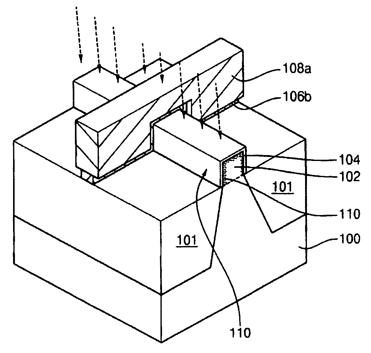
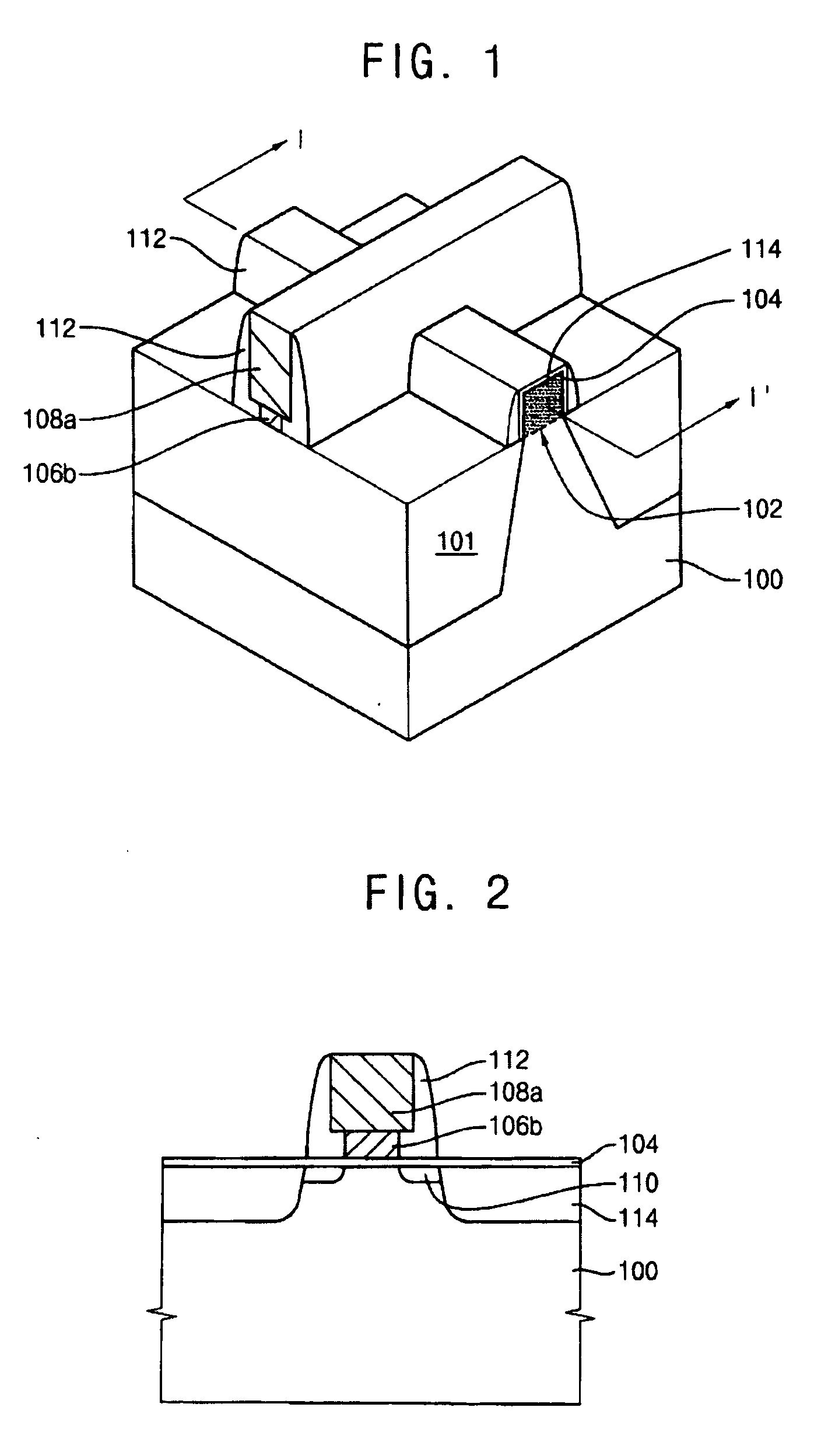
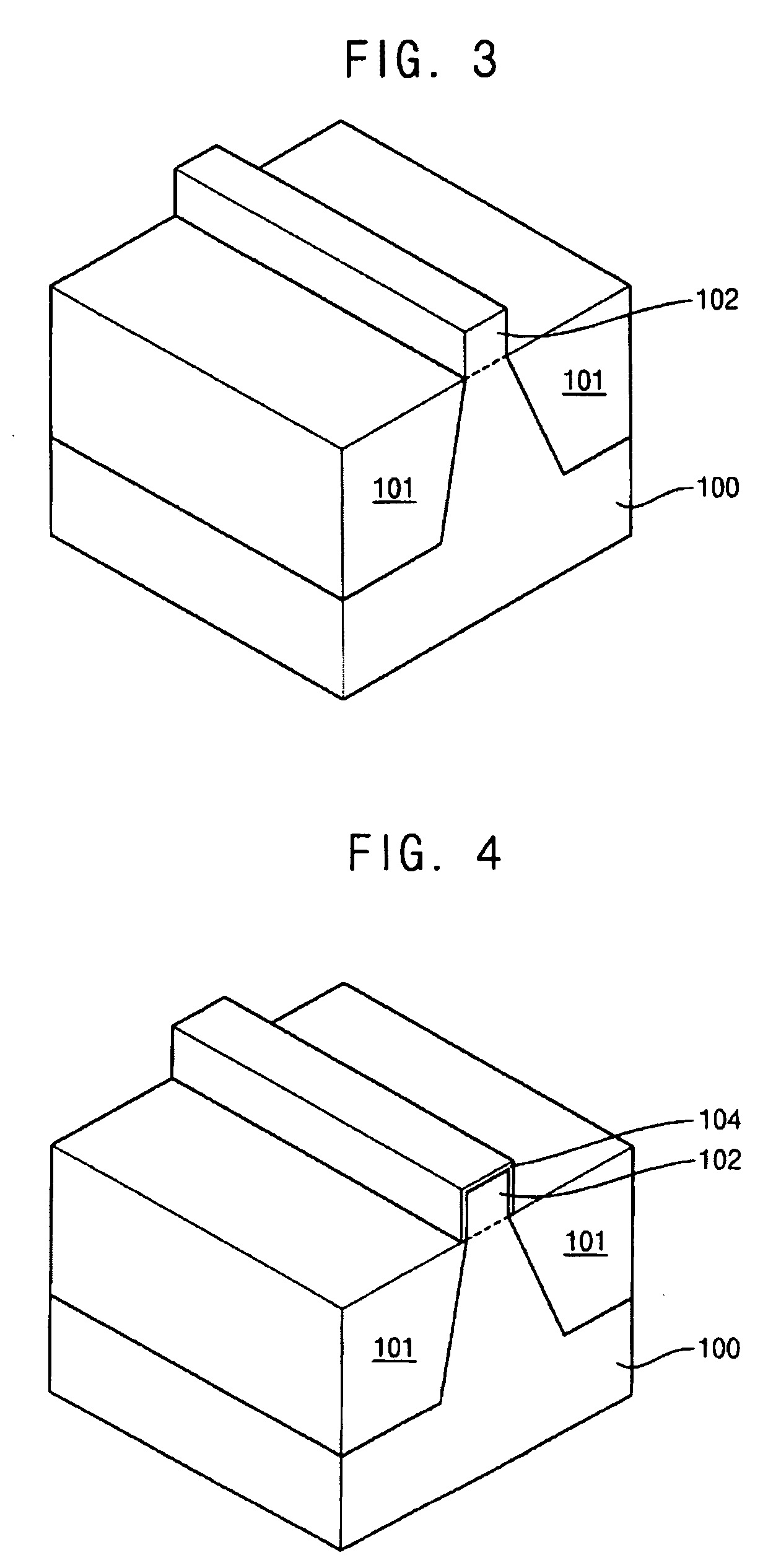
[0009]Example embodiments provide a fin field effect transistor (FinFET) that is capable of reducing a gate induced drain leakage (GIDL) current with increased capacity. Example embodiments also provide a method of manufacturing the above-mentioned FinFET.
[0024]According to example embodiments, the FinFET may have the source / drain expansion regions having a uniform doping concentration in the surface of the active fin. Thus, the FinFET may have improved capacity. Further, the source / drain expansion regions may not excessively infiltrate into an edge of the first electrode pattern. Therefore, the areas of the gate electrode and the source / drain expansion regions may not overlap with each other much, so that the GIDL current may be reduced.

Problems solved by technology

However, in a planar MOSFET, an electrical field may affect the planar MOSFET by a drain voltage because the channel length may become shorter.
Further, this may cause a short channel effect where a channel drive capacity may be deteriorated due to a gate electrode.
However, this may cause relatively low mobility of carriers and a relatively low current drive force.
Therefore, in the planar MOSFET, suppressing the short channel effect may be difficult because the planar MOSFET may have a more rapid operational speed and an increased integration degree.
However, because a body width of the fin is gradually narrowed and the fin has the three-dimensional shape, the surface of the fin may not be readily doped with impurities.
As a result, the GIDL current may not be sufficiently reduced.
Further, a higher energy to dope the sidewall of the fin with the impurities through the offset spacer may be required which causes damages to the surface of the fin.

Method used


Image

  • Fin field effect transistor and method of manufacturing the same
  • Fin field effect transistor and method of manufacturing the same
  • Fin field effect transistor and method of manufacturing the same

Examples


Embodiment Construction

[0032]Example embodiments are described more fully hereinafter with reference to the accompanying drawings, in which example embodiments are shown. Example embodiments may, however, be embodied in many different forms and should not be construed as limited to example embodiments set forth herein. Rather, these example embodiments are provided so that this disclosure will be thorough and complete, and will fully convey the scope of example embodiments to those skilled in the art. In the drawings, the sizes and relative sizes of layers and regions may be exaggerated for clarity.

[0033]It will be understood that when an element or layer is referred to as being “on,”“connected to” or “coupled to” another element or layer, it can be directly on, connected or coupled to the other element or layer or intervening elements or layers may be present. In contrast, when an element is referred to as being “directly on,”“directly connected to” or “directly coupled to” another element or layer, ther...


PUM


Abstract

Provided are a FinFET and a method of manufacturing the same. A FinFET may include at least one active fin, at least one gate insulating layer pattern, a first electrode pattern, a second electrode pattern and at least one pair of source / drain expansion regions. The at least one active fin may be formed on a substrate. The at least one gate insulating layer pattern may be formed on the at least one active fin. The first electrode pattern may be formed on the at least one gate insulating layer pattern. Further, the first electrode pattern may be intersected with the at least one active fin. The second electrode pattern may be formed on the first electrode pattern. Further, the second electrode pattern may have a width greater than that of the first electrode pattern. The at least one pair of source / drain expansion regions may be formed on a surface of the at least one active fin on both sides of the first electrode pattern. Thus, the FinFET may have improved capacity and reduced GIDL current.

Description

PRIORITY STATEMENT[0001]This application claims priority under 35 U.S.C. §119 to Korean Patent Application No. 2007-88162, filed on Aug. 31, 2007, in the Korean Intellectual Property Office (KIPO), the entire contents of which are herein incorporated by reference.BACKGROUND[0002]1. Field[0003]Example embodiments relate to a field effect transistor, and a method of manufacturing the same. Other example embodiments relate to a fin field effect transistor (FinFET), and a method of manufacturing the FinFET.[0004]2. Description of the Related Art[0005]In order to provide semiconductor devices with a more rapid operational speed and increased integration degree, a channel length of a MOS field effect transistor (MOSFET) has been gradually reduced. However, in a planar MOSFET, an electrical field may affect the planar MOSFET by a drain voltage because the channel length may become shorter. Further, this may cause a short channel effect where a channel drive capacity may be deteriorated due...

Claims


Application Information

Patent Timeline
Patent Type & Authority Applications(United States)
IPC IPC(8): H01L29/00H01L21/336H01L21/8238H01L27/092H01L29/423H01L29/49H01L29/78H01L29/786
CPCH01L29/4925H01L29/7856H01L29/66795H01L29/4958H01L29/42376H01L29/49H01L29/785
Inventor KIM, SUNG-MINKIM, MIN-SANGLEE, JI-MYOUNGKIM, DONG-WON
Owner SAMSUNG ELECTRONICS CO LTD
Why Eureka
Try Eureka