Thermally enhanced thin semiconductor package

a technology of semiconductor die package and thermal enhancement, which is applied in the direction of semiconductor device details, semiconductor/solid-state device devices, electrical devices, etc., can solve the problems of defective manufacturing of semiconductor die package, failure of semiconductor die package formation, and need for rework

Inactive Publication Date: 2009-03-05
SEMICON COMPONENTS IND LLC
View PDF67 Cites 21 Cited by
  • Summary
  • Abstract
  • Description
  • Claims
  • Application Information

AI Technical Summary

Problems solved by technology

Another technical challenge that exists is in the formation of such semiconductor die packages.
If the clip and the leadframe are not properly

Method used


Image

  • Thermally enhanced thin semiconductor package
  • Thermally enhanced thin semiconductor package
  • Thermally enhanced thin semiconductor package

Examples


Embodiment Construction

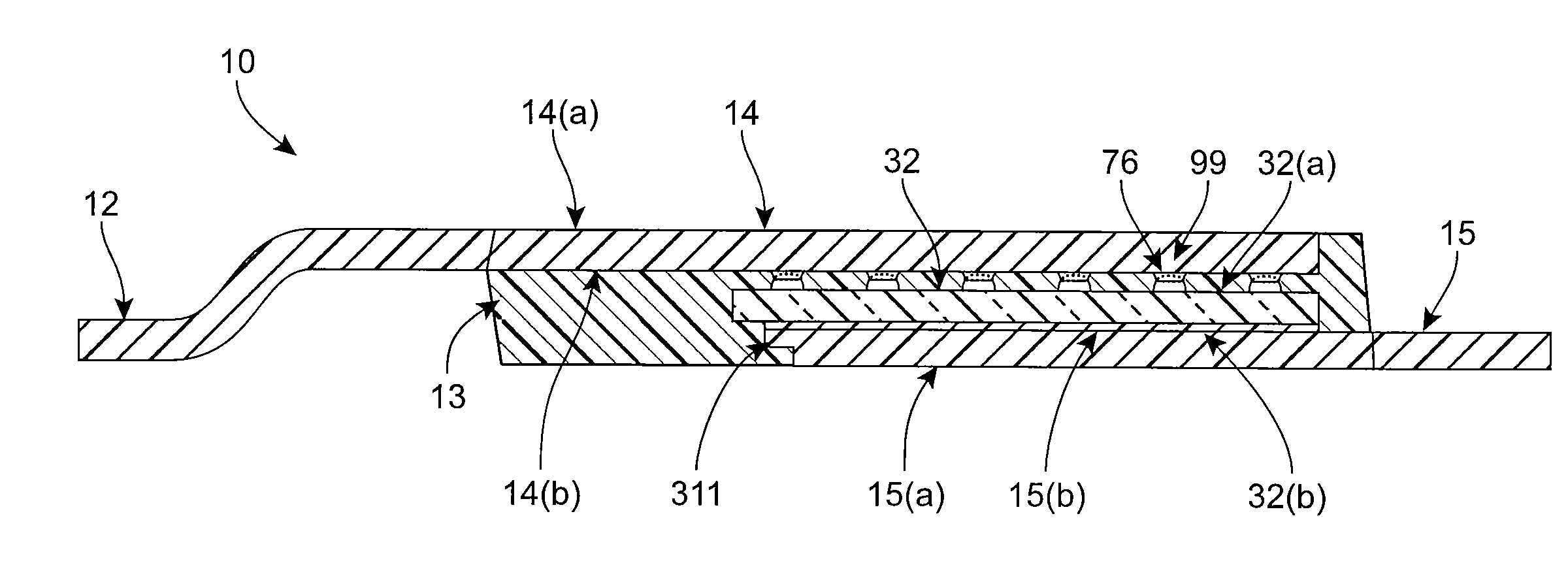
[0031]One embodiment of the invention is directed to a semiconductor die package. The semiconductor die package includes a semiconductor die comprising an input (e.g., a source region) at a first top semiconductor die surface and an output (e.g., a drain region) at a second bottom semiconductor die surface. A leadframe having a first leadframe surface and a second leadframe surface opposite the first leadframe surface is in the semiconductor die package and is coupled to the first top semiconductor die surface. A clip (e.g., a drain clip) having a first clip surface and a second clip surface is coupled to the second bottom semiconductor die surface. A molding material having exterior molding material surfaces covers at least a portion of the leadframe, the clip, and the semiconductor die. The first leadframe surface and the first clip surface are exposed by the molding material, and the first leadframe surface, the first clip surface, and the exterior molding material surfaces of th...


PUM


Abstract

A semiconductor die package is disclosed. The semiconductor die package includes a semiconductor die comprising an input at a first top semiconductor die surface and an output at a second bottom semiconductor die surface. A leadframe having a first leadframe surface and a second leadframe surface opposite the first leadframe surface is in the semiconductor die package and is coupled to the first top semiconductor die surface. A clip having a first clip surface and a second clip surface is coupled to the second bottom semiconductor die surface. A molding material having exterior molding material surfaces covers at least a portion of the leadframe, the clip, and the semiconductor die. The first leadframe surface and the first clip surface are exposed by the molding material, and the first leadframe surface, the first clip surface, and the exterior molding material surfaces of the molding material form exterior surfaces of the semiconductor die package.

Description

CROSS-REFERENCES TO RELATED APPLICATIONS[0001]Not ApplicableBACKGROUND[0002]Semiconductor die packages are known in the semiconductor industry, but could be improved. For example, electronic devices such as wireless phones and the like are becoming smaller and smaller. It is desirable to make thinner semiconductor die packages so that they can be incorporated into such electronic devices. It would also be desirable to improve upon the heat dissipation properties of conventional semiconductor die packages.[0003]Another technical challenge that exists is in the formation of such semiconductor die packages. A clip and a leadframe may sandwich a semiconductor die in an exemplary semiconductor die package. If the clip and the leadframe are not properly aligned with each other and the semiconductor die, then the manufactured semiconductor die package could be defective and rework may be needed.[0004]Embodiments of the invention address these and other problems, individually and collective...

Claims


Application Information

Patent Timeline
IPC IPC(8): H01L23/495H01L21/56
CPCH01L23/4334H01L23/49524H01L2924/1305H01L2924/1306H01L2924/10253H01L2224/73253H01L2224/32245H01L2224/16245H01L2924/0665H01L2924/014H01L2924/01019H01L2924/01006H01L23/49562H01L23/544H01L24/33H01L24/40H01L24/81H01L24/83H01L2223/54433H01L2223/54473H01L2224/1134H01L2224/13111H01L2224/13147H01L2224/81193H01L2224/8121H01L2224/81815H01L2224/83801H01L2924/01005H01L2924/01013H01L2924/01029H01L2924/01033H01L2924/01047H01L2924/01078H01L2924/01079H01L2924/01082H01L2924/13091H01L2924/18301H01L2224/2919H01L2924/00H01L2924/181H01L2224/84801H01L2224/37124H01L2224/37147H01L2224/3754H01L2224/371H01L24/37H01L2224/0603H01L24/84H01L2924/00012H01L2924/00014H01L23/28H01L23/48
Inventor MADRID, RUBEN P.
Owner SEMICON COMPONENTS IND LLC
Why Eureka
Try Eureka