Semiconductor device and fabrication method for same

a semiconductor and fabrication method technology, applied in semiconductor devices, solid-state devices, printed circuit aspects, etc., can solve the problems of reduced emission efficiency of led devices, ineffective dissipation of heat, and increased heat generation in a larger amount, so as to achieve superior heat resistance, heat dissipation, and durability.

Active Publication Date: 2014-11-06
SHIKOKU INSTR
View PDF7 Cites 64 Cited by
  • Summary
  • Abstract
  • Description
  • Claims
  • Application Information

AI Technical Summary

Benefits of technology

[0061]With the present invention, since the layer in which almost all of components are made of inorganic materials can be formed on the substrate, the semiconductor device can be provided which includes the electrical insulating layer with superior heat resistance, heat dissipation, and durability.
[0062]Furthermore, since the electrical insulating layer serves as a reflecting material, an expensive reflecting material is no longer required even when the semicon...

Problems solved by technology

In trying to increase the emission intensity of the LED device, heat generates in a larger amount, and the emission efficiency of the LED device reduces with heating.
However, known structures employing the ceramic substrate or the silicon substrate have the problems that heat is not effectively dissipated because ceramics and silicon have lower thermal conductivity than metals, such as copper, that those substrates are relatively expensive, and that a difficulty occurs in processing of the substrates.
Thus, it is known to use the heat-resistant and thermoplastic resin as the insulating layer, but the insulating layer made of the resin has a problem with heat dissipation.
Moreover, heat dissipa...

Method used


Image

  • Semiconductor device and fabrication method for same
  • Semiconductor device and fabrication method for same
  • Semiconductor device and fabrication method for same

Examples


Embodiment Construction

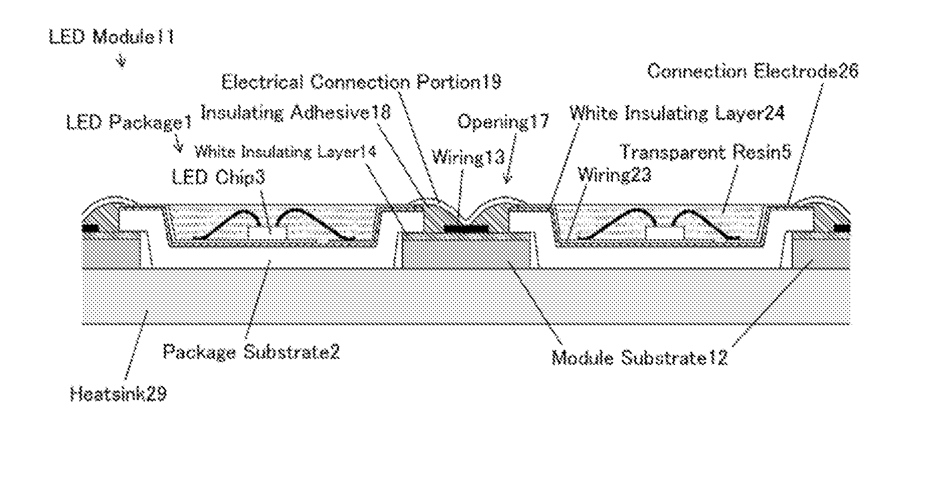
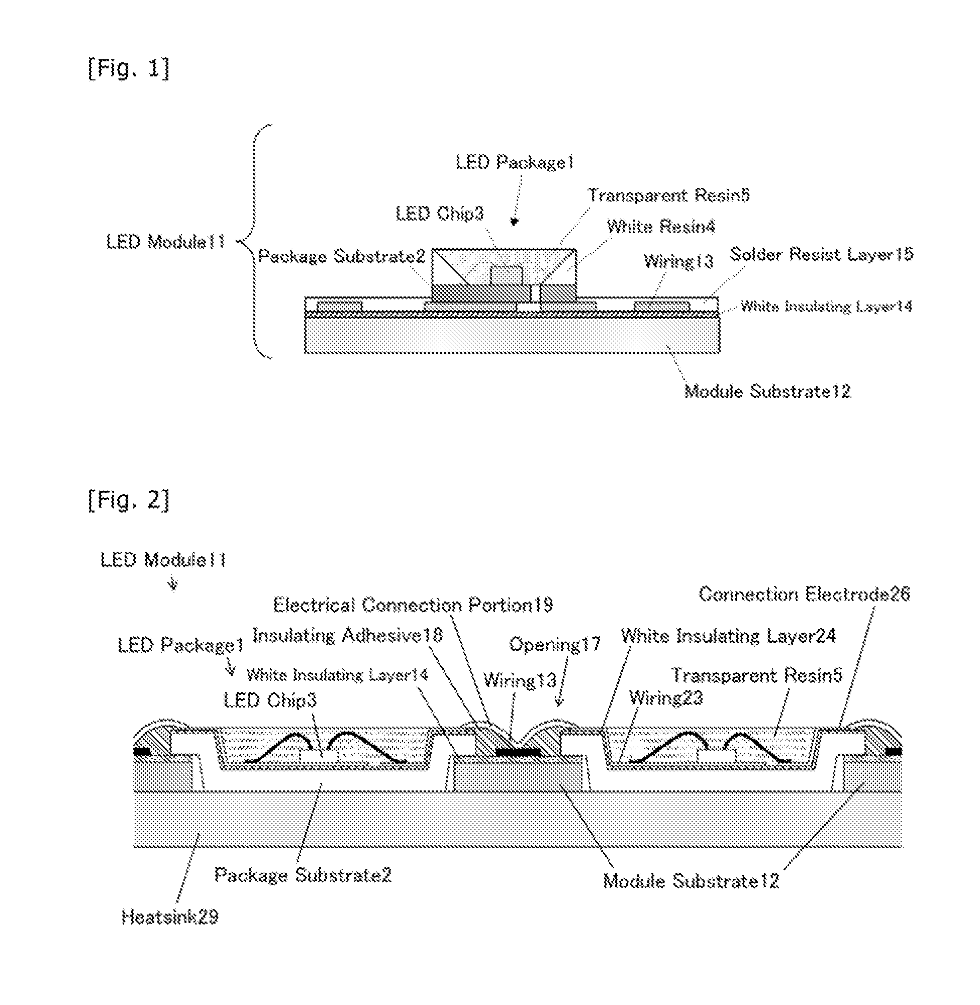
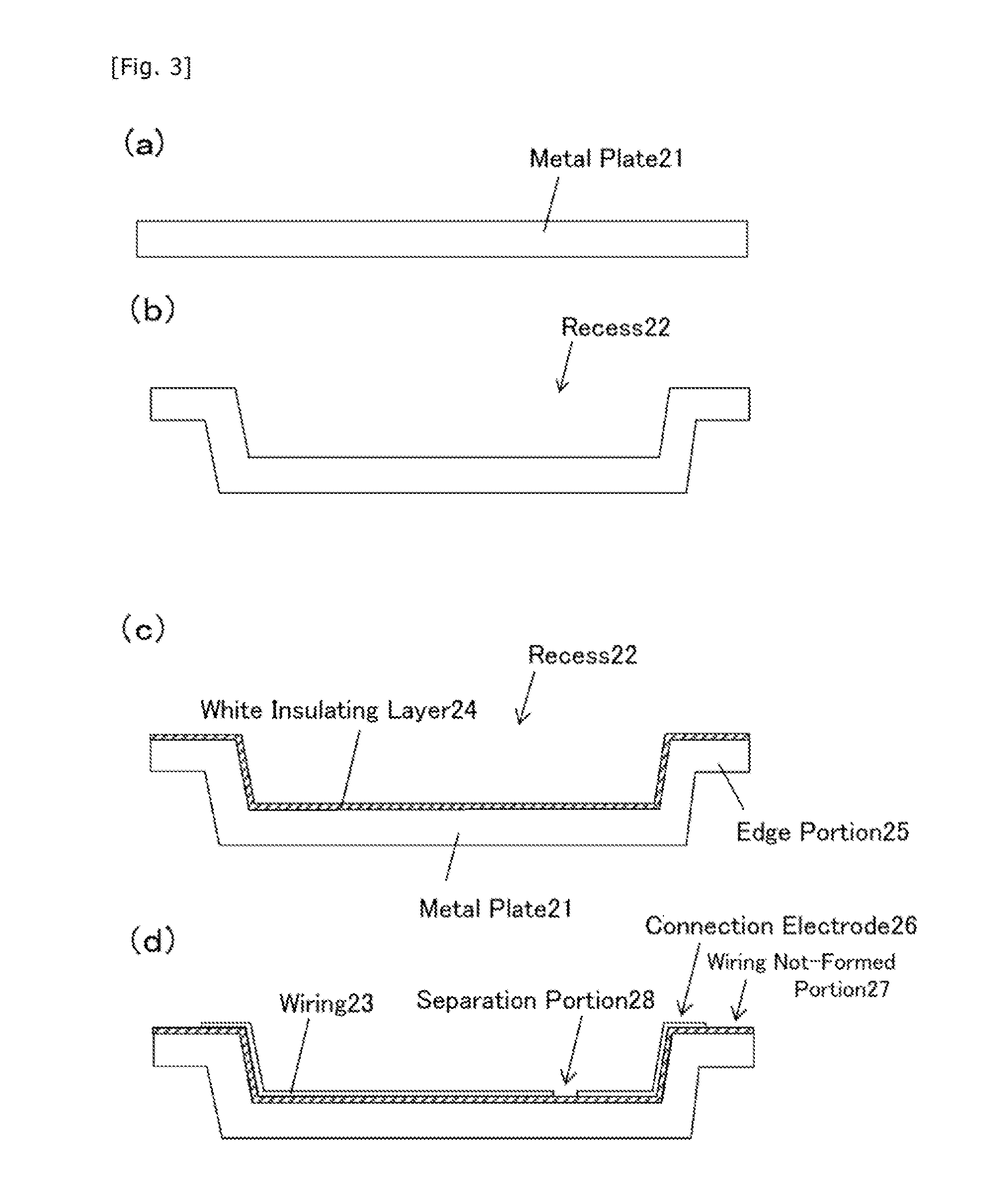
[0089]The present invention will be described below in connection with exemplary embodiments. FIG. 1 is a side sectional view illustrating a first configuration example of an LED illumination module embodying the present invention. An LED illumination module 11 of FIG. 1 includes, as main components, a known LED package 1, and a module substrate 12 on which a wiring 13 and a white insulating layer 14 are formed.

[0090]The LED package 1 is constituted by fixing and electrically connecting an LED chip 3 to a package substrate 2, and then encapsulating the LED chip 3 with a transparent resin 5 (e.g., an epoxy-based or silicone-based resin). The LED package 1 is mounted such that electrodes disposed on the backside of the package substrate 2 are connected to the wiring 13 formed on the module substrate 12 by soldering, for example. A luminescent surface of the LED chip 3 faces upwards as viewed in FIG. 1, and emits light upwards without being blocked by the package substrate 2.

[0091]Whil...


PUM


Abstract

A semiconductor device includes an electrical insulating layer with superior heat resistance, heat dissipation, and durability, and which is manufactured through a process with good cost performance and process performance. In a semiconductor device including a first substrate to which a semiconductor chip is mounted directly or indirectly, and a white insulating layer formed on a surface of the first substrate and functioning as a reflecting material, the semiconductor chip is an LED, at least the surface of the first substrate is made of a metal, and a stacked structure of the white insulating layer and a metal layer is formed by coating a liquid material, which contains SiO2 in the form of nanoparticles and a white inorganic pigment, over the surface of the first substrate and baking the coated liquid material.

Description

TECHNICAL FIELD[0001]The present invention relates to a semiconductor device including a white inorganic insulating layer that functions as a reflecting material and that is superior in heat resistance, heat dissipation, and durability, and to a manufacturing method for the semiconductor device. More particularly, the present invention relates to an LED luminescent device including a white insulating layer that is formed, for example, by coating a liquid material, which contains SiO2 in the form of nanoparticles and a white inorganic pigment, over a metal surface and baking the coated liquid material, and to a manufacturing method for the LED luminescent device.BACKGROUND ART[0002]An LED (Light Emitting Diode) is widely used as a device having low power consumption, contributing to reduction of carbon dioxide, and exhibiting high durability, namely as a device that contributes to environmental protection and energy saving. A package incorporating such an LED chip is mounted onto a w...

Claims


Application Information

Patent Timeline
IPC IPC(8): H01L33/60
CPCH01L33/60H01L24/97H01L25/0753H01L33/62H01L2224/16225H01L2224/48091H01L2224/48227H01L2924/12041H01L2224/97H01L2924/01029H01L2224/81H01L2224/85H01L2924/00014H01L2224/48228H01L2924/07802H05K1/056H01L2224/48137H01L2224/73265H05K2201/0209H05K2201/10106H05K2201/2054H01L2924/15747H01L2924/15787H01L2924/181H01L2924/12042H01L2924/00H01L2924/00012
Inventor ISHIHARA, MASAMICHIOYAMA, KENSHUMURAKAMI, SHOJIONOSAKA, HITONOBU
Owner SHIKOKU INSTR
Why Eureka
Try Eureka