LED package

Active Publication Date: 2009-09-10
SEOUL SEMICONDUCTOR
View PDF5 Cites 67 Cited by
  • Summary
  • Abstract
  • Description
  • Claims
  • Application Information

AI Technical Summary

Benefits of technology

[0011]Accordingly, an object of the present invention is to provide an LED package, wherein one cavity for defining a circumference of an LED chip and other cavities necessary for exposing lead frames are separately formed in a supporting member for supporting lead frames, and the cavity defining the circumference of the LED chip is separatel

Problems solved by technology

The reason is that when heat generated from the LED chip remains for a long period of time, dislocation and mismatch occur in a crystal structure of the LED chip.
However, in the conventional LED package, since the heat sink slug has a volume relatively larger than a heat sink area through which the heat sink slug is exposed to the outside, its use is restricted if the heat sink slug is not made of a expensive thermal conductive material.
Further, there is a problem in that much cumbersomeness in a process may occur when mounting the heat sink slug.
Furthermore, the heat sink slug may become a cause of hindering compactness of the LED package.
However, in the conventional LED package, since the first resin portion is formed by injecting

Method used


Image

  • LED package
  • LED package
  • LED package

Examples


embodiment

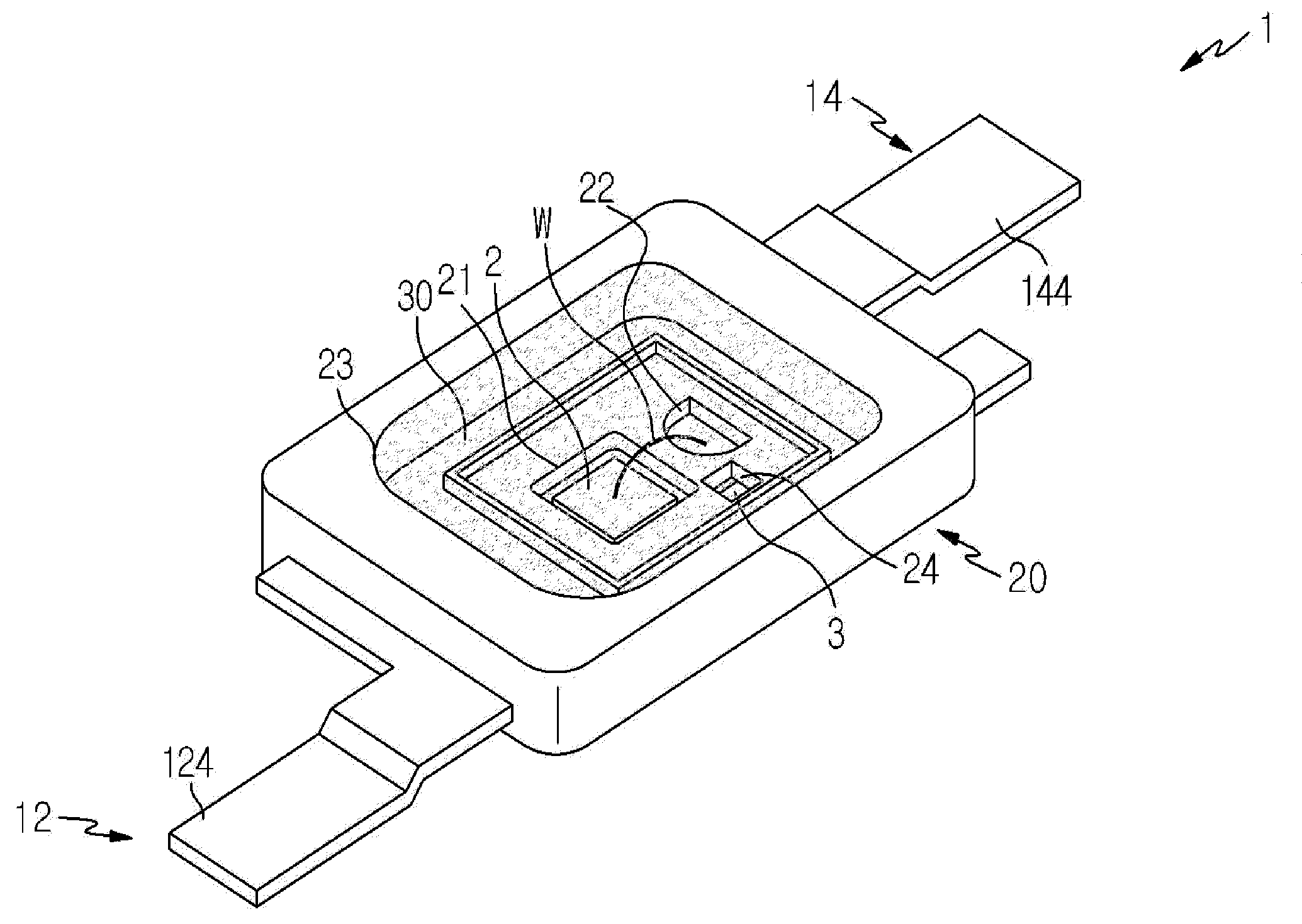
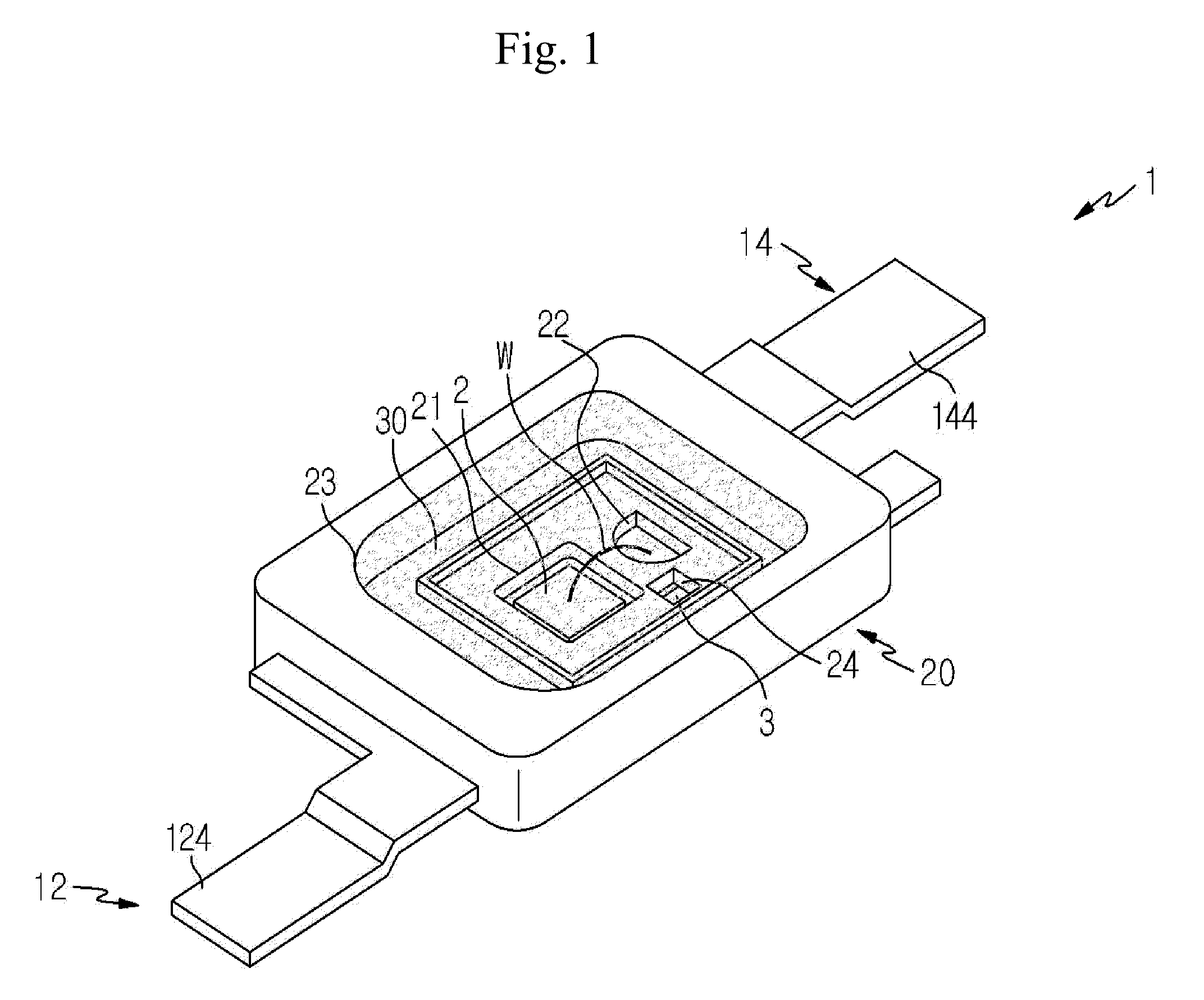
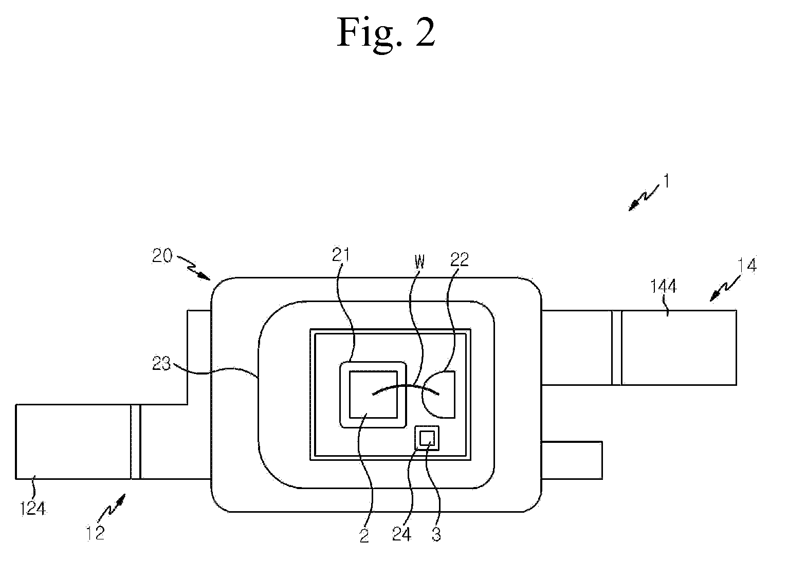
[0023]FIG. 1 is a perspective view showing an LED package according to an embodiment of the present invention; FIG. 2 is a plan view showing the LED package according to the embodiment of the present invention from which a molding member is removed; FIG. 3 is a sectional view of the LED package according to the embodiment of the present invention; FIG. 4 is a perspective view illustrating the configuration of a lead frame according to the embodiment of the present invention.

[0024]Referring to FIGS. 1 to 3, an LED package 1 of this embodiment comprises an LED chip 2; first and second lead frames 12 and 14 for applying current to the LED chip 2; a member 20 for supporting the first and second lead frames 12 and 14 (hereinafter, referred to as a “supporting member”); and a transparent molding member 30 (shown in FIGS. 1 and 3) formed to protect the LED chip 2.

[0025]Referring to FIGS. 3 and 4, each of the first and second lead frames 12 and 14 has the shape of a long plate made of a met...


PUM


Abstract

The present invention relates a light emitting diode (LED) package. The present invention provides an LED package, wherein one cavity for defining a circumference of an LED chip and other cavities necessary for exposing lead frames are separately formed in a supporting member for supporting lead frames, and the cavity defining the circumference of the LED chip is separately filled with a resin, whereby it is possible to prevent an irregular interface between the resin portions, and when a phosphor is contained in the resin portion formed to be confined in the circumference of the LED chip, it is possible to reduce color deviation for each light directional angle and to prevent unnecessary waste of the phosphor.
To this end, an LED package according to the present invention comprises first and second lead frames disposed to be spaced apart from each other; an LED chip mounted on the first lead frame and connected to the second lead frame by a bonding wire; a supporting member formed to support the first and second lead frames, the supporting member defining first and second cavities divided from each other, the first cavity being formed on the first lead frame having the LED chip positioned thereon, the second cavity being formed on the second lead frame having one end of the bonding wire positioned thereon; and a molding member including a first resin portion filled in the first cavity to cover the LED chip and a second resin portion covering the first resin portion while a portion of the second resin is filled in the second cavity.

Description

CROSS REFERENCE TO RELATED APPLICATIONS[0001]This application claims priority from and the benefit of Korean Patent Application No. 10-2007-0032017, filed on Mar. 30, 2007, which is hereby incorporated by reference for all purposes as if fully set forth herein.BACKGROUND OF THE INVENTION[0002]1. Field of the Invention[0003]The present invention relates to a light emitting diode (LED) package, and more particularly, to an LED package including lead frames on which an LED chip is mounted and a supporting member for supporting the lead frames, wherein the structure of the supporting member, and furthermore, the structure of lead frames are improved.[0004]2. Description of the Related Art[0005]An LED is an element in which electrons or holes are combined in a P-N semiconductor junction structure by application of current thereby emitting certain light. The LED is typically formed to have a package structure, in which an LED chip is mounted, and is frequently referred to as an “LED packa...

Claims


Application Information

Patent Timeline
IPC IPC(8): H01L33/00H01L33/48H01L33/54H01L33/62
CPCH01L33/483H01L33/54H01L33/62H01L2924/01322H01L2224/48091H01L2924/00014
Inventor SEO, JUNG HOOKANG, SUK JIN
Owner SEOUL SEMICONDUCTOR
Why Eureka
Try Eureka