Optical information recording medium and recording film for optical information recording medium
a technology of optical information and recording medium, which is applied in the direction of data recording, record carrier materials, instruments, etc., can solve the problems of media not always reading and the super-rens disk mentioned above requires a higher readout power, so as to achieve a lower readout power and lower readout power
- Summary
- Abstract
- Description
- Claims
- Application Information
AI Technical Summary
Benefits of technology
Problems solved by technology
Method used
Image
Examples
example 1
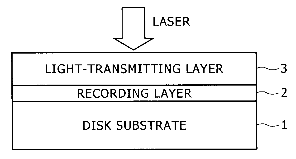
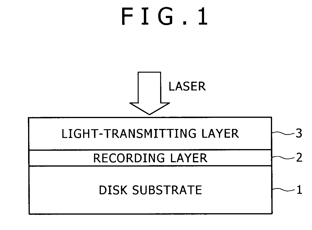
[0033]The optical information recording medium (optical disk) pertaining to Example 1 has a structure as shown in FIG. 1. It was prepared in the following manner.
[0034]First, the disk substrate 1, which is a polycarbonate sheet, 1.1 mm thick, having a track pitch of 0.32 μm, a groove width of 0.16 μm, and a groove depth of 25 nm, is coated by DC sputtering (under the conditions shown below) with the metal thin film 2 (as the recording film) which has the composition shown in Table 1 (determined by ICP analysis).
[0035]Target for sputtering: pure In or pure Sn, with a metal chip of Co, Ni, or Bi placed thereon.
[0036]Ultimate pressure: lower than 10−5 Torr (1 Torr=133.3 Pa)
[0037]Total pressure of sputtering gas: 3 mTorr
[0038]DC sputtering power: 25 to 100 W (as shown in Table 1).
[0039]The recording layer (recording film) varies in thickness as shown in Table 1.
[0040]The recording layer 2 was spin-coated with a UV-curable resin (“BRD-130” from NIPPON KAYAKU CO., LTD.). Upon curing, the ...
example 2
[0053]This example is intended to measure the C / N ratio for short recording marks longer than those in Example 1. A detailed description follows.
[0054]An optical disk having the structure shown in FIG. 1 was prepared in the following manner.
[0055]First, the disk substrate 1, which is a polycarbonate sheet, 1.1 mm thick, having a track pitch of 0.32 μm, a groove width of 0.16 μm, and a groove depth of 25 nm, is coated by DC sputtering (under the conditions shown below) with the metal thin film 2 of an alloy having a composition of In-47.1Co-1.8Sn.
[0056]Target for sputtering: pure In or pure Sn, with a Co chip placed thereon.
[0057]Ultimate pressure: not higher than 10−5 Torr Total pressure of sputtering gas: 3 mTorr
[0058]DC sputtering power: 100 W
[0059]The recording layer 2 has a thickness of 12 nm.
[0060]The recording layer 2 was spin-coated with a UV-curable resin (“BRD-130” from NIPPON KAYAKU CO., LTD.). Upon curing, the resin layer turned into the light-transmitting layer 3 having ...
PUM
| Property | Measurement | Unit |
|---|---|---|
| wavelength | aaaaa | aaaaa |
| wavelength | aaaaa | aaaaa |
| length | aaaaa | aaaaa |
Abstract
Description
Claims
Application Information

