Method for fabricating pixel structure
- Summary
- Abstract
- Description
- Claims
- Application Information
AI Technical Summary
Benefits of technology
Problems solved by technology
Method used
Image

Examples
Embodiment Construction
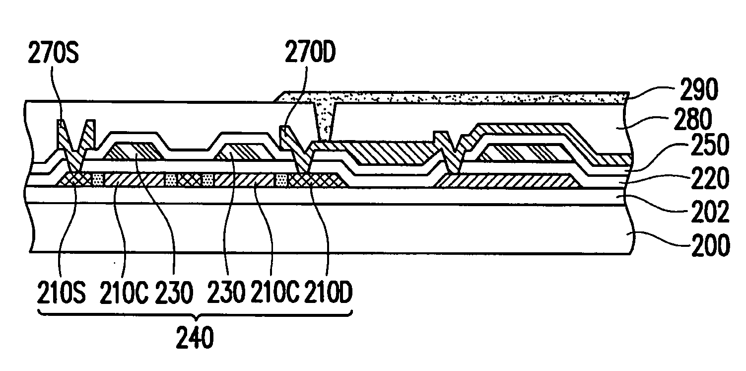
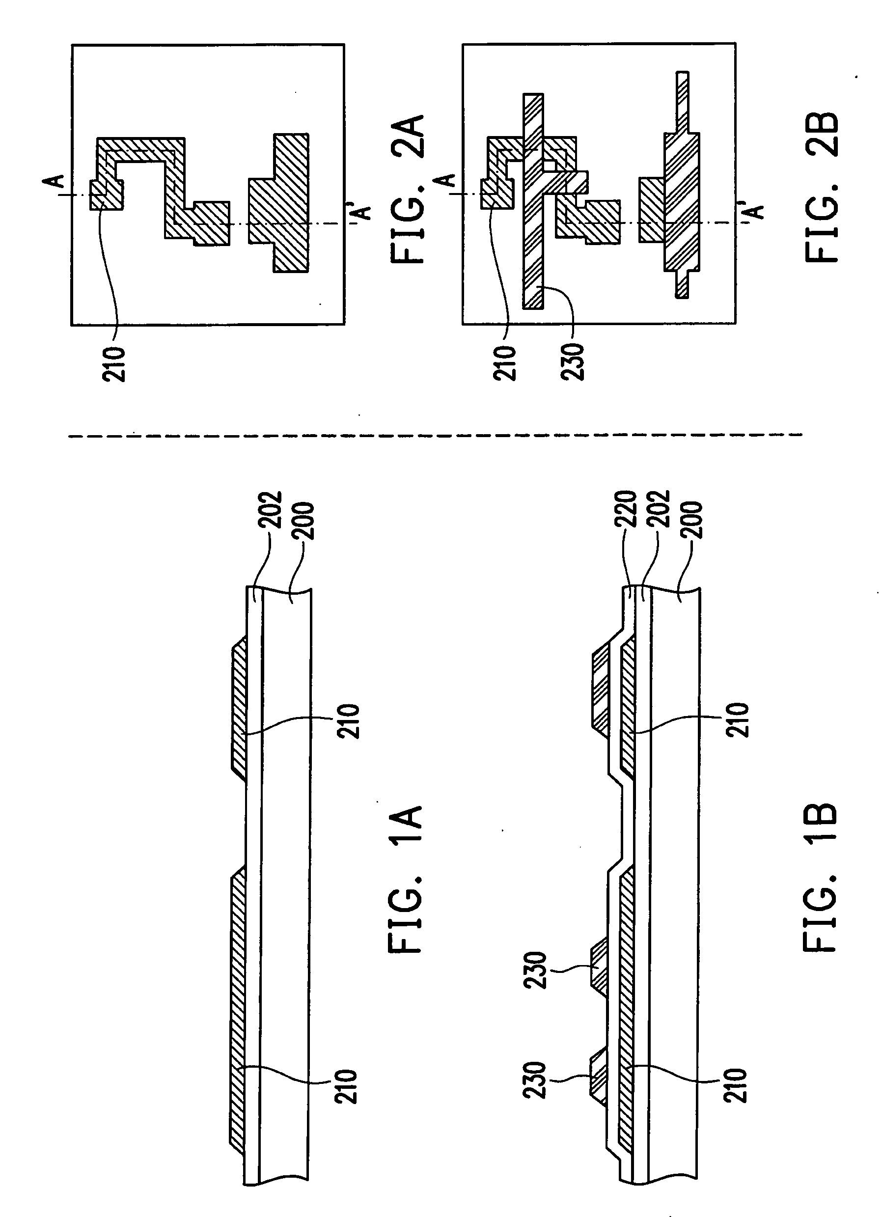
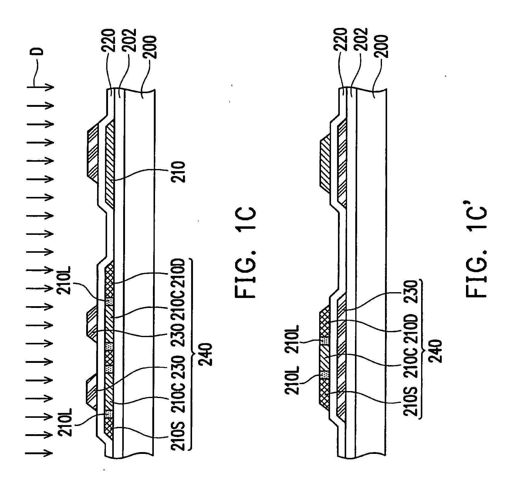
[0027]FIGS. 1A to 1I are schematic cross-sectional views for illustrating a method for fabricating a pixel structure of the present invention. Referring to FIG. 1A, first, a substrate 200 is provided, and the substrate 200 is, for example, a rigid substrate or a flexible substrate, such as, glass substrate or plastic substrate. Then, a semiconductor layer 210 is formed on the substrate 200. In this embodiment, the method for forming the semiconductor layer 210 includes the following steps. First, a semiconductor material layer (not shown) is formed on the substrate 200. Then, the semiconductor material layer is patterned by a photolithography process and an etching process, so as to form a semiconductor layer 210. FIG. 2A is a top view of FIG. 1A, and FIG 1A is a cross-sectional view taken along a section line of A-A′ of FIG. 2A. In addition, the material of the semiconductor layer 210 is, for example, poly-silicon or doped poly-silicon.
[0028]In this embodiment, before forming the s...
PUM
 Abstract
Description
Claims
Application Information
 - R&D Engineer
- R&D Manager
- IP Professional
- Industry Leading Data Capabilities
- Powerful AI technology
- Patent DNA Extraction
Browse by: Latest US Patents, China's latest patents, Technical Efficacy Thesaurus, Application Domain, Technology Topic.
© 2024 PatSnap. All rights reserved.Legal|Privacy policy|Modern Slavery Act Transparency Statement|Sitemap