
Buffered Memory Module Supporting Two Independent Memory Channels

a memory module and buffer technology, applied in the field of data processing systems, can solve the problems of increasing the package size of a system, affecting the performance of the memory module, so as to increase the memory bandwidth through the memory module and double the storage capacity of the memory modul

Inactive Publication Date: 2009-03-05
IBM CORP
View PDF99 Cites 46 Cited by
  • Summary
  • Abstract
  • Description
  • Claims
  • Application Information

AI Technical Summary

Benefits of technology

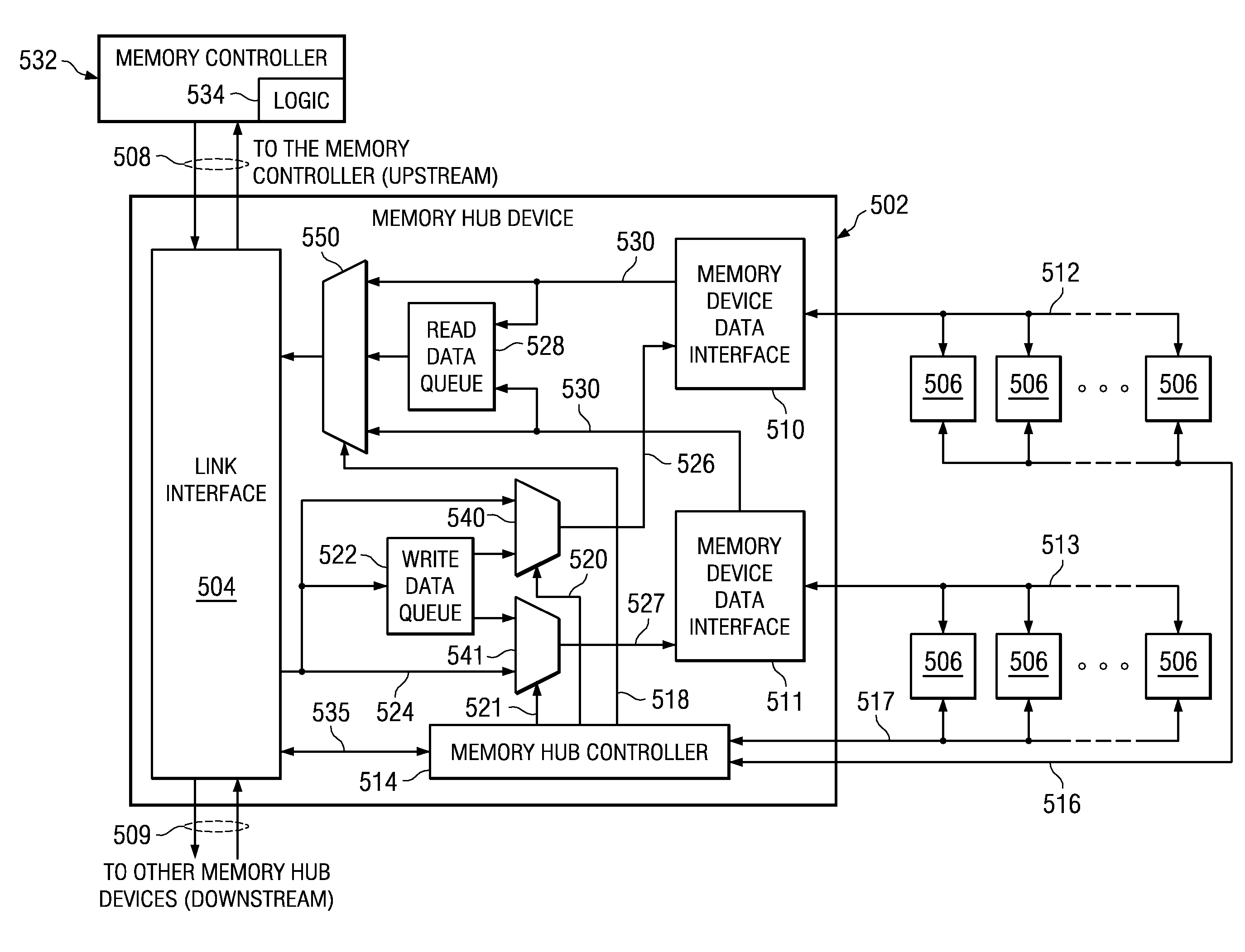
[0010]In order to increase the memory bandwidth through a memory module, the illustrative embodiments implement multiple memory device data interfaces in a memory hub device of a memory module that interfaces between a memory controller of a processor and memory devices on the memory module. Providing multiple memory device data interfaces on the memory hub device results in a more even match between the bandwidth on a memory channel coupled to the memory module and the bandwidth of the memory device data interface of a single memory module. Additionally, the multiple memory device data interfaces on the memory hub device also double the storage capacity of the memory module.
[0011]The illustrative embodiments provide mechanisms for enhancing the memory bandwidth available through a buffered memory module. One illustrative embodiment provides multiple memory device data interfaces in a memory hub device of a memory module that interfaces between a memory controller of a processor and memory devices on the memory module. Another illustrative embodiment provides for using a high-frequency, high-bandwidth point-to-point interface or memory channel that generally connects a memory hub device to another memory module in a daisy-chain configuration as an independent memory channel onto the memory module. A further illustrative embodiment provides a memory module stacking implementation that pins out data buses of two stacked four-bit wide memory devices separately but electrically connects the chip select signals of the two four-bit wide memory devices together for parallel access.

Problems solved by technology

High-availability systems present further challenges as related to overall system reliability due to customer expectations that new computer systems will markedly surpass existing systems in regard to mean-time-before-failure (MTBF), in addition to offering additional functions, increased performance, increased storage, lower operating costs, etc.
Other frequent customer requirements further exacerbate the memory system design challenges, and include such items as ease of upgrade and reduced system environmental impact, such as space, power, and cooling.
In a dense computing environment where there may be hundreds of processor racks, increasing the package size for a system may not be a viable option.
The bandwidth capability of the memory channel that is feeding the DIMM is significantly larger than the bandwidth capability of the interface to the DRAMs on the DIMM creating a mismatch of bandwidths.
A mismatch of bandwidths normally results in loss of performance in the system.
That is, even though the processor is able to send access requests to the memory hub device using the high-bandwidth memory channel, the memory hub device is limited in its access to the DRAMS by lower-bandwidth memory interface.
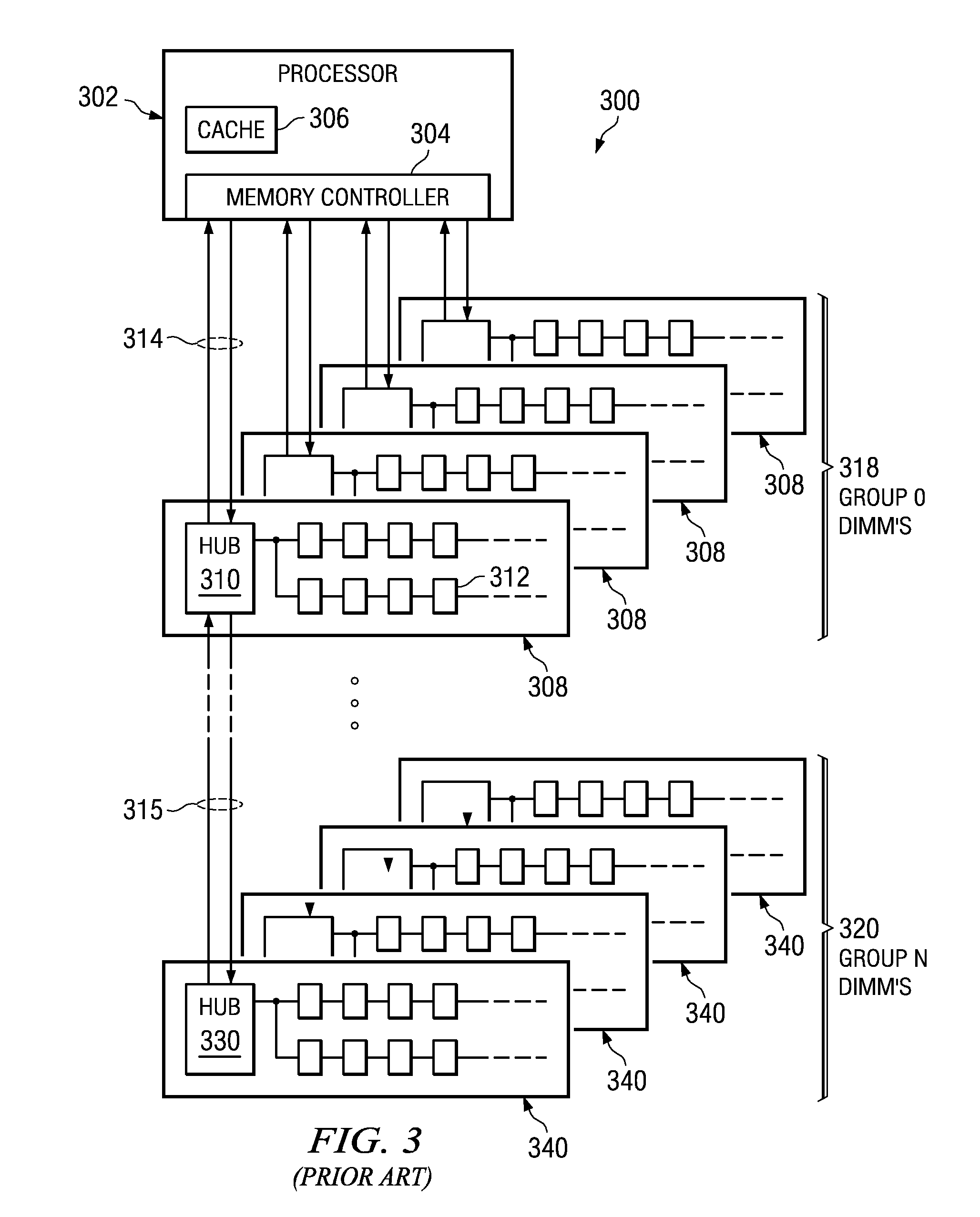
However, the link between the memory hub devices results in added latency on read operations, which results in lower system performance.
Additionally, there are many system configurations that do not have the physical space for a second DIMM socket.
Without the space for the second socket there is no solution to efficiently use the bandwidth on the memory channel.
In addition, for systems that target very dense computing environments, there may not be enough DIMM connectors for all the memory channels on the processor interface, let alone providing multiple DIMMs per memory channel.

Method used


Image

  • Buffered Memory Module Supporting Two Independent Memory Channels
  • Buffered Memory Module Supporting Two Independent Memory Channels
  • Buffered Memory Module Supporting Two Independent Memory Channels

Examples


Embodiment Construction

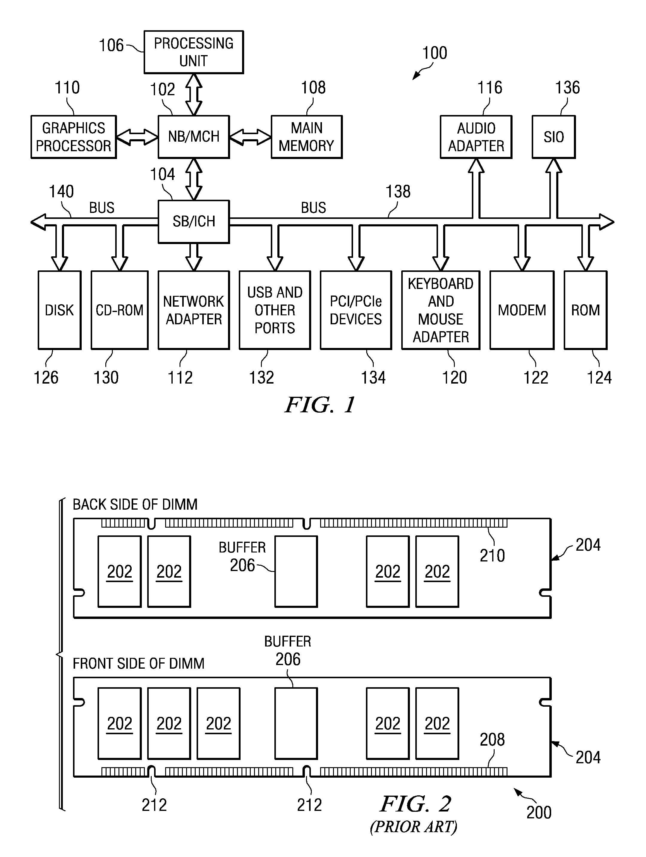
[0028]The illustrative embodiments provide mechanisms for enhancing the memory bandwidth available through a buffered memory module. As such, the mechanisms of the illustrative embodiments may be used with any of a number of different types of data processing devices and environments. For example, the memory system of the illustrative embodiments may be utilized with data processing devices such as servers, client data processing systems, stand-alone data processing systems, or any other type of data processing device. Moreover, the memory systems of the illustrative embodiments may be used in other electronic devices in which memories are utilized including printers, facsimile machines, storage devices, flashdrives, or any other electronic device in which a memory is utilized. In order to provide a context for the description of the mechanisms of the illustrative embodiments, and one example of a device in which the illustrative embodiments may be implemented, FIG. 1 is provided he...


PUM


Abstract

A memory system is provided that enhances the memory bandwidth available through a memory module. The memory system includes a memory controller and a memory module coupled to the memory controller. In the memory system, the memory controller is coupled to the memory module via at least two independent memory channels. In the memory system, the at least two independent memory channels are coupled to one or more memory hub devices of the memory module.

Description

GOVERNMENT RIGHTS[0001]This invention was made with Government support under DARPA, HR0011-07-9-0002. THE GOVERNMENT HAS CERTAIN RIGHTS IN THIS INVENTION.BACKGROUND[0002]1. Technical Field[0003]The present application relates generally to an improved data processing system. More specifically, the present application is directed to a buffered memory module supporting two independent memory channels.[0004]2. Description of Related Art[0005]Contemporary high performance computing main memory systems are generally composed of one or more dynamic random access memory (DRAM) devices, which are connected to one or more processors via one or more memory control elements. Overall computer system performance is affected by each of the key elements of the computer structure, including the performance / structure of the processor(s), any memory cache(s), the input / output (I / O) subsystem(s), the efficiency of the memory control function(s), the main memory device(s), and the type and structure of ...

Claims


Application Information

Patent Timeline
Patent Type & Authority Applications(United States)
IPC IPC(8): G06F12/00
CPCG06F13/1668
Inventor GOWER, KEVIN C.MAULE, WARREN E.
Owner IBM CORP
Learn More