

Semiconductor device and manufacturing method thereof
a technology of semiconductor devices and semiconductors, applied in the direction of semiconductor devices, basic electric elements, electrical equipment, etc., can solve the problems of difficult manufacturing of miniaturized devices, adverse effects on transistor characteristics, and dramatic fluctuation of voltage (vth) of pmosfets, so as to reduce the non-uniformity of threshold voltage
- Summary
- Abstract
- Description
- Claims
- Application Information
AI Technical Summary
Benefits of technology
Problems solved by technology
Method used
Image

Examples
Embodiment Construction
[0033]The preferred embodiments of the present invention will be described in detail below with reference to the accompanying drawings.
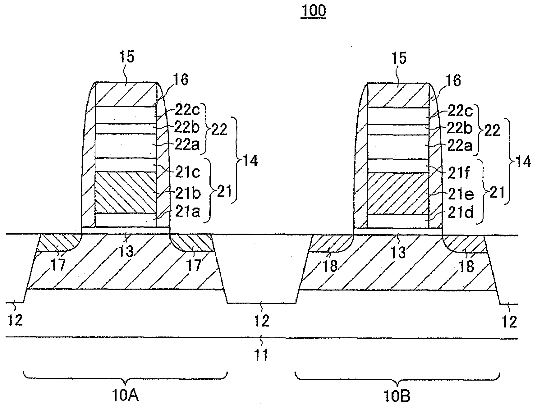
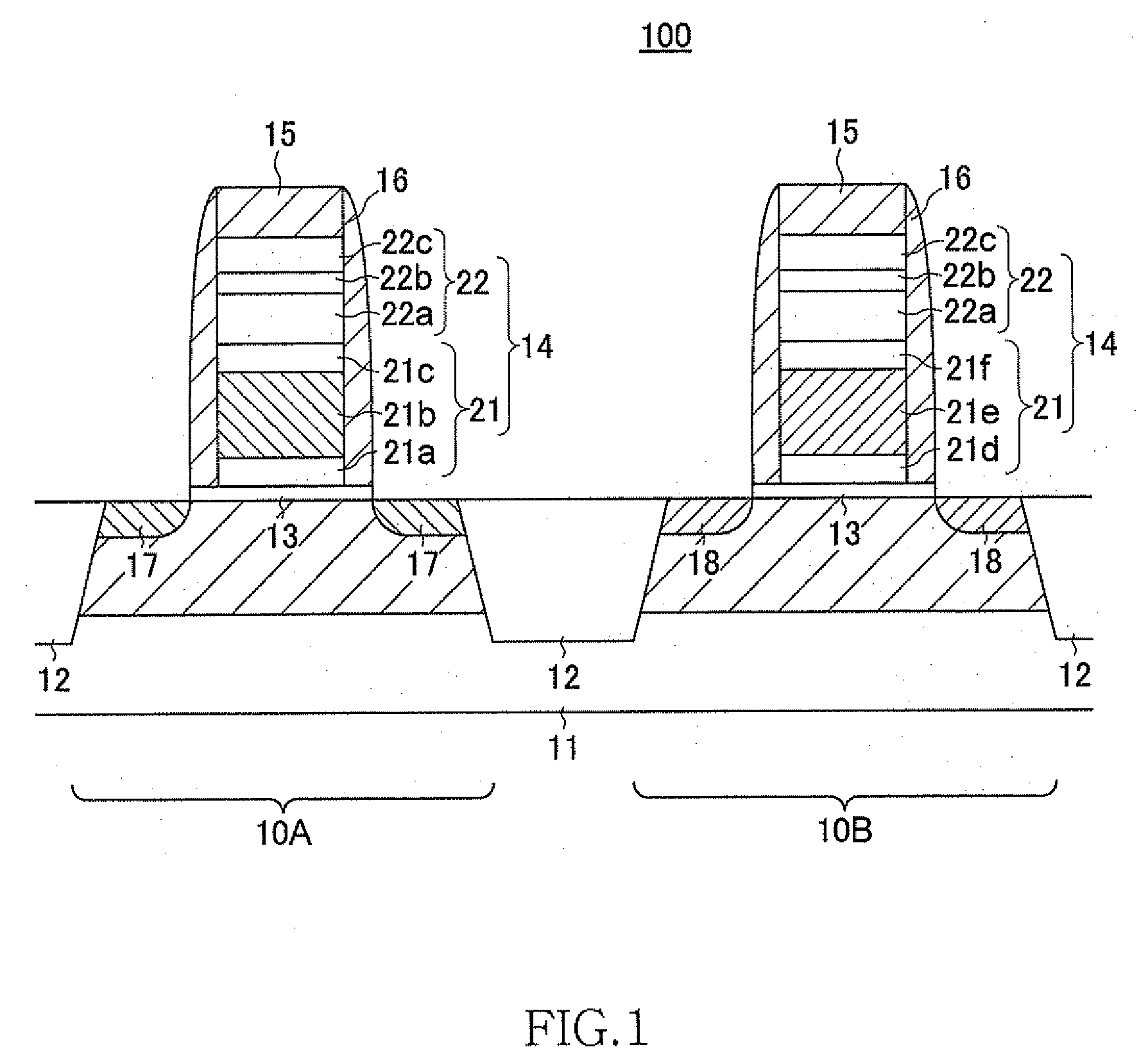
[0034]FIG. 1 is a schematic cross-sectional view showing the structure of the semiconductor device 100 according to a preferred embodiment of the present invention.
[0035]The semiconductor device 100 is a dual-gate CMOS in which a NMOSFET 10A having an n+ polysilicon gate and a PMOSFET 10B having a p+ polysilicon gate are formed on the same substrate, as shown in FIG. 1. The NMOSFET 10A and the PMOSFET 10B are both provided with a gate insulation film 13 formed on a silicon substrate 11, a gate electrode 14 formed on the gate insulation film 13, a gate cap insulation film 15 that covers the top surface of the gate electrode 14, sidewall insulation films 16 that covers side surfaces of the gate electrode 14, first diffusion layers 17 that serve as source / drain regions for the NMOSFET 10A, and second diffusion layers 18 that serve as source / drain region...
PUM
 Abstract
Description
Claims
Application Information