Semiconductor device, lead frame, and microphone package therefor

a semiconductor device and lead frame technology, applied in the direction of semiconductor electrostatic transducers, casings/cabinets/drawers, casings/cabinets/drawers details, etc., can solve the problem of electromagnetic noise entering the cavity, and achieve the effect of improving the shield effect of the semiconductor device and the microphone packag

Inactive Publication Date: 2009-03-12
YAMAHA CORP
View PDF3 Cites 12 Cited by
  • Summary
  • Abstract
  • Description
  • Claims
  • Application Information

AI Technical Summary

Benefits of technology

[0010]It is an object of the present invention to provide a semiconductor device, which is designed to reduce gaps allowing electromagnetic noise to enter into a cavity by use of resin mold technology, thus achieving shield performance substantially equivalent to that of a ceramic package.

Problems solved by technology

The aforementioned semiconductor device suffers from a gap between the periphery of the stage and the cover and gaps between the leads adjoining together, wherein these gaps are not completely covered with the stage and the cover.
Hence, it is likely that electromagnetic noise may enter into the cavity via the gaps.

Method used


Image

  • Semiconductor device, lead frame, and microphone package therefor
  • Semiconductor device, lead frame, and microphone package therefor
  • Semiconductor device, lead frame, and microphone package therefor

Examples


Embodiment Construction

[0042]The present invention will be described in further detail by way of examples with reference to the accompanying drawings.

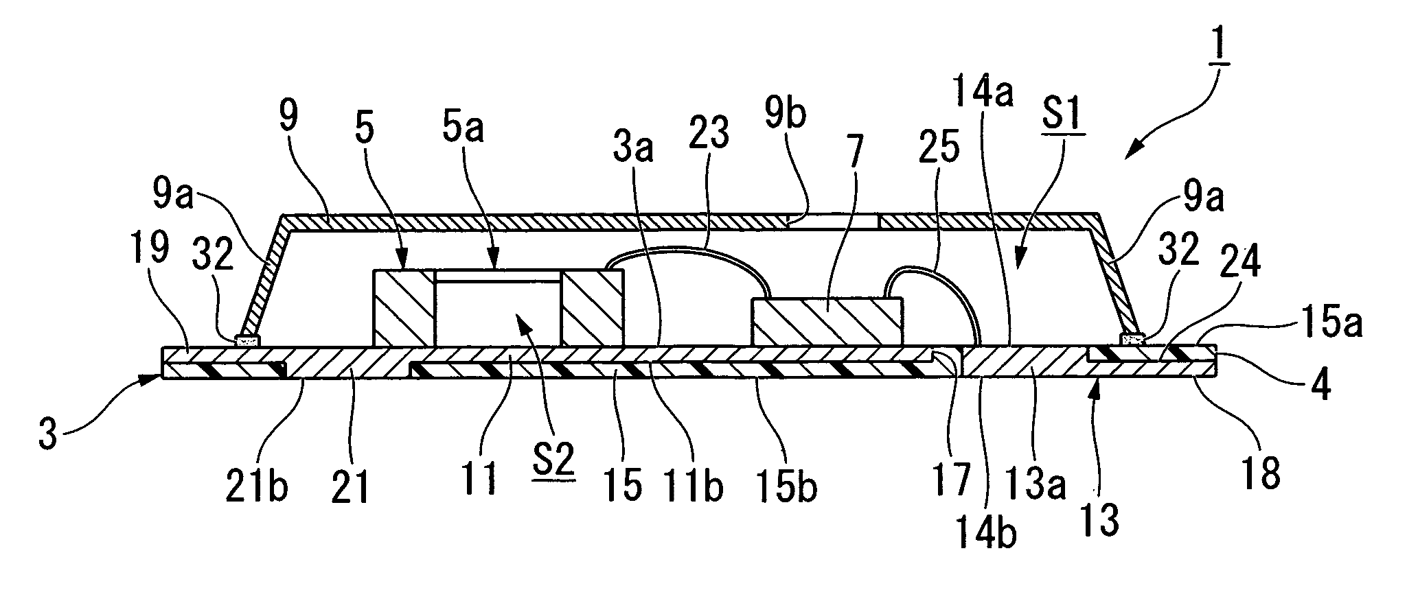
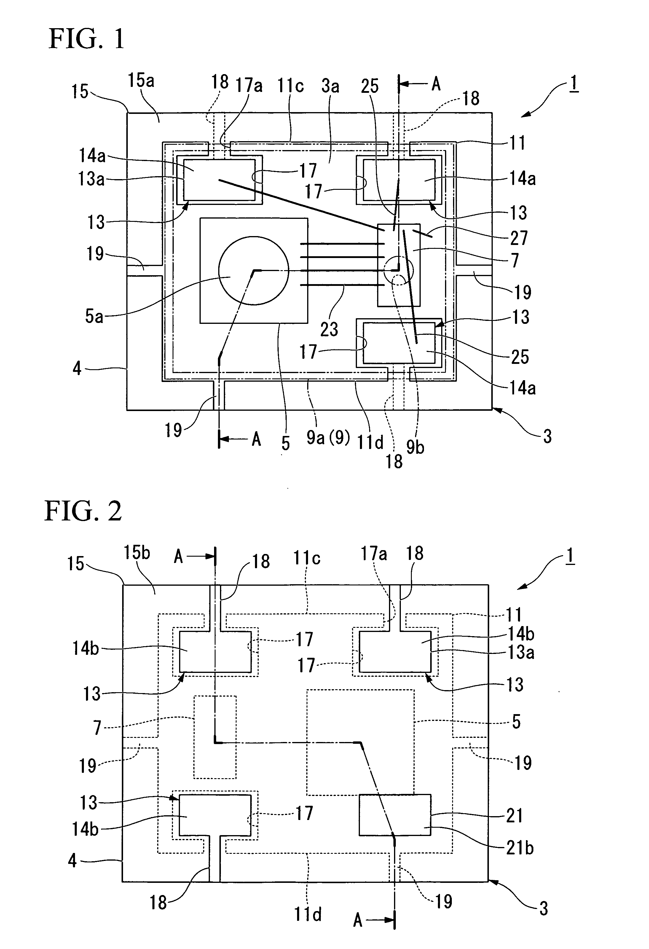
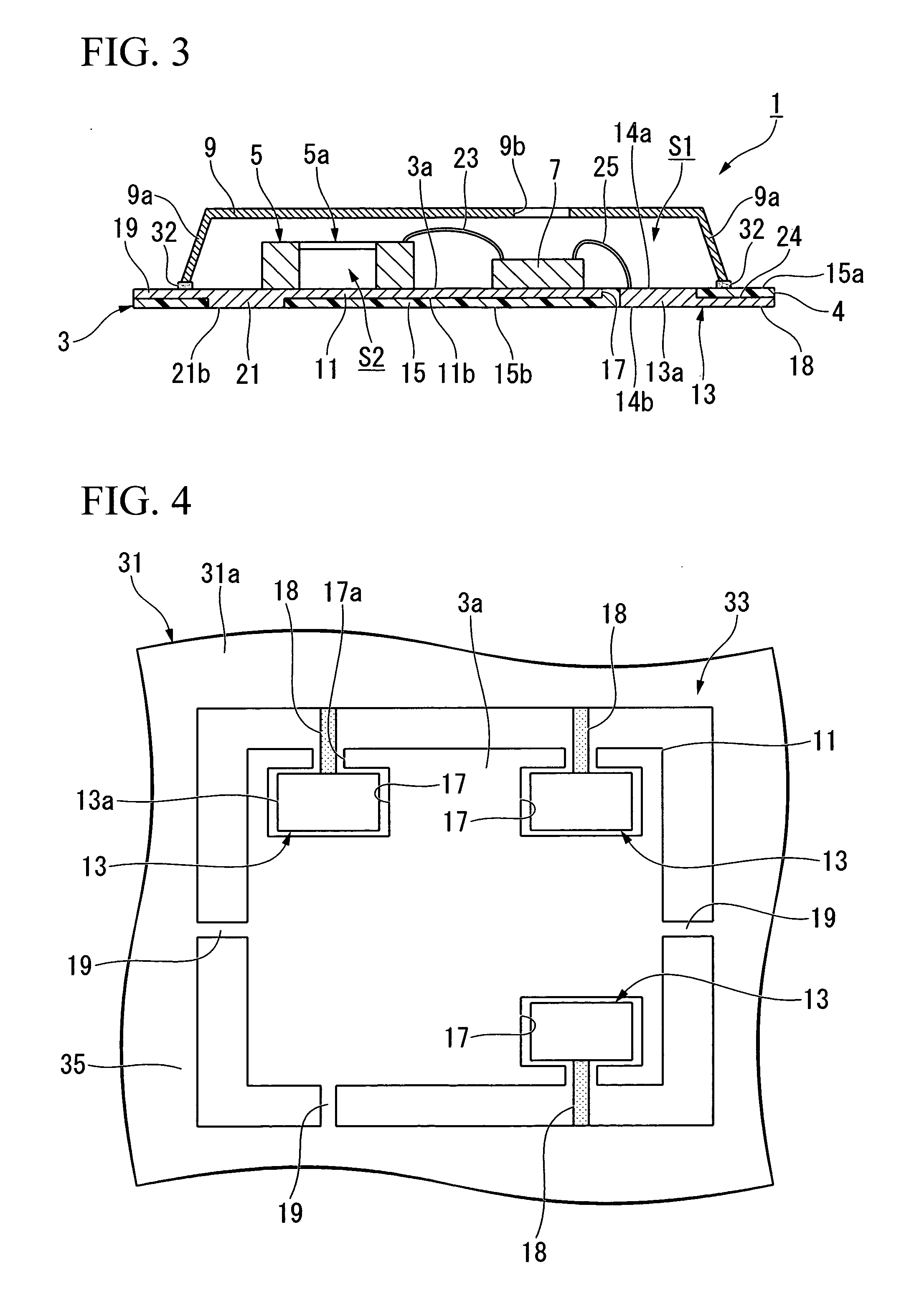
[0043]A semiconductor device 1 according to a preferred embodiment of the present invention will be described with reference to FIGS. 1 to 8. The semiconductor device 1 is designed to detect variations of pressures such as sound pressures generated in the external space and is a surface mount type produced using a lead frame.

[0044]As shown in FIGS. 1 to 3, the semiconductor device 1 is constituted using a mold sheet 3 having a rectangular shape in a plan view, a microphone chip (or a sensor chip) 5 and a companion chip 7 formed on a surface 3a of the mold sheet 3, and a cover 9 which is arranged above the mold sheet 3 so as to cover the microphone chip 5 and the companion chip 7.

[0045]The mold sheet 3 is constituted of a stage 11 which has a rectangular shape in a plan view so as to form the surface 3a of the mold sheet 3, a plurality of lead terminals (e.g....


PUM


Abstract

A semiconductor device is constituted of a mold sheet for mounting a sensor chip and a cover having a box-like shape, both of which are combined together so as to form a cavity therebetween. The mold sheet includes a stage having a rectangular shape in a plan view, a plurality of cutouts formed in the periphery of the stage, and a plurality of lead terminals arranged inside of the cutouts. The lead terminals include a plurality of connection portions electrically connected to the sensor chip and a plurality of support leads which are externally extended from the periphery of the stage. The stage and the lead terminals are sealed with a mold resin, by which they are electrically insulated from each other. The recesses of the support leads are sealed with the insulating resin mold relative to the surface of the mold sheet so as to mount the opening end of the cover.

Description

BACKGROUND OF THE INVENTION[0001]1. Field of the Invention[0002]The present invention relates to semiconductor devices having sensor chips and lead frames, which are encapsulated in microphone packages.[0003]The application claims priority on Japanese Patent Application No. 2007-206724, the content of which is incorporated herein by reference.[0004]2. Description of the Related Art[0005]In conventionally-known semiconductor devices, sensor chips (for sensing sounds and the like) are incorporated into the hollow cavities defined by substrates and covers and are mounted on the surfaces of substrates. Various types of semiconductor devices have been disclosed in various documents such as Patent Document 1.[0006]Patent Document 1: Japanese Unexamined Patent Application Publication No. 2007-66967[0007]Patent Document 1 teaches a semiconductor device having a substrate which includes a rectangular stage for mounting a sensor chip thereon, a plurality of leads arranged in the surrounding a...

Claims


Application Information

Patent Timeline
Patent Type & Authority Applications(United States)
IPC IPC(8): H01L29/84H05K7/12
CPCH04R19/005H05K5/0095H01L2224/48091H01L2224/48137H01L2224/49175H01L2924/3025H01L2224/48247H01L2924/00014H01L2924/00H01L2924/16151H01L2924/16152H01L23/02H04R19/04H01L21/56
Inventor SHIRASAKA, KENICHI
Owner YAMAHA CORP
Why Eureka
Try Eureka