Micro-Emitter Array Based Full-Color Micro-Display

a micro-emitter array and full-color technology, applied in the field of micro-emitter array based full-color micro-display, can solve the problems of low power efficiency, limited field of view, brightness, and contrast of modulation-based micro-display, and inorganic counterparts with inferior power efficiency and lifetim

Active Publication Date: 2009-03-26
III N TECH
View PDF4 Cites 229 Cited by
  • Summary
  • Abstract
  • Description
  • Claims
  • Application Information

AI Technical Summary

Benefits of technology

[0015]Additionally, tunneling junctions are inserted into the InGaN-based structures for the purpose of avoiding problems encountered in plasma-etching. Further, an electrical connection can be made between a first n-contact associated with the AlGaInP-based structures and a second n-contact, the second n-contact being deposed on an n-GaN layer which is deposed between a green emissive layer and a blue emissive layer; the n-GaN layer, green emissive layer, and blue emissive layer all being included in the InGaN-based structures; the first and second contacts together creating a common-grounded anode; a first cathode associated with and electrically controlling the red emitter; a second cathode associated with and electrically controlling the green emitter; and a third cathode associated with and electrically controlling the blue emitter. In this embodiment, an order of stacking of the emitters includes the red emitter being deposed proximate the substrate, the green emitter being deposed above the red emitter, and the blue emitter being deposed above the green emitter, the red, green, and blue light emissions being directed away from the substrate to contribute to a multicolor display.

Problems solved by technology

These modulating microdisplays are blanket illuminated by separate light sources and modulate incident light on a pixel-by-pixel basis, with intrinsically low power efficiency.
Due at least in part to this mode of operation, the field-of-view, brightness, and contrast of these modulation-based microdisplays are limited.
Although dramatic progress has been made in the OLED field in the last 20 years, the electro-optical performance, power efficiency and lifetime of OLEDs themselves are still inferior to their inorganic counterparts, LEDs.
OLED microdisplays suffer not only from a shorter life span but also from nonuniform degradation of luminance for various colors over their lifespan.
Furthermore, because of technical difficulties such as conflicting temperatures that may be required for growth of different color organic thin films, and incompatibility with conventional photolithography micro-patterning processes, full-color OLED microdisplays with high resolution based on side-by-side patterned RGB sub-pixels have not been demonstrated.
In such a case, the OLED must be driven up to ten times brighter than the required pixel brightness, which substantially shortens a lifetime of the microdisplay.
Furthermore, since the fabrication of certain semiconductor emitters may not be compatible with the silicon integrated circuits that provide the current needed to light up, or drive an LED, a / k / a “driver” IC chips, microdisplays formed from such emitters cannot be directly constructed on such IC chips.

Method used


Image

  • Micro-Emitter Array Based Full-Color Micro-Display
  • Micro-Emitter Array Based Full-Color Micro-Display
  • Micro-Emitter Array Based Full-Color Micro-Display

Examples


Embodiment Construction

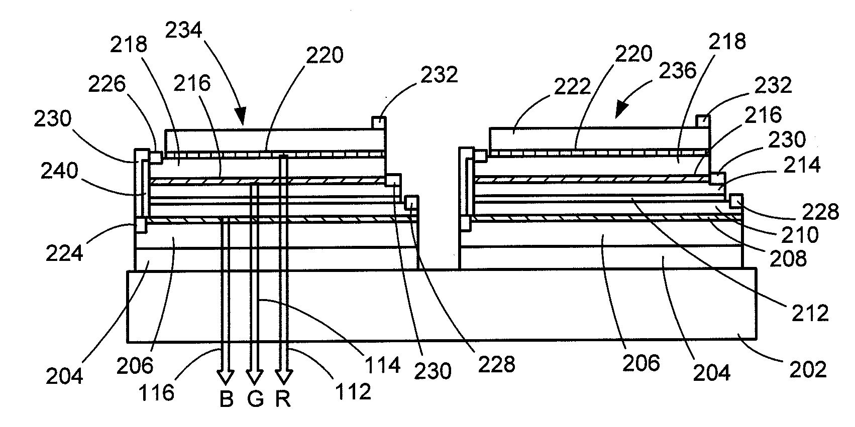
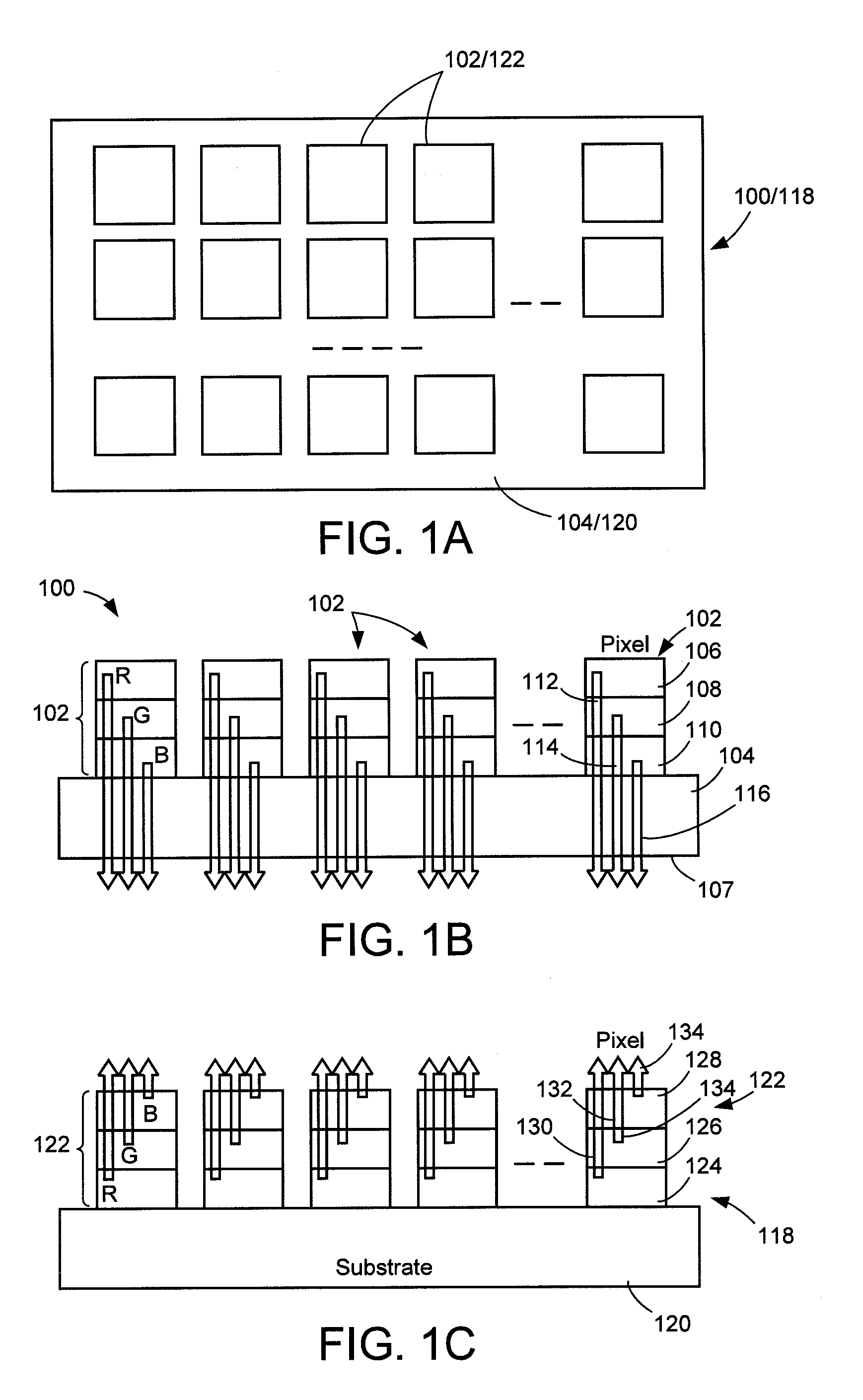
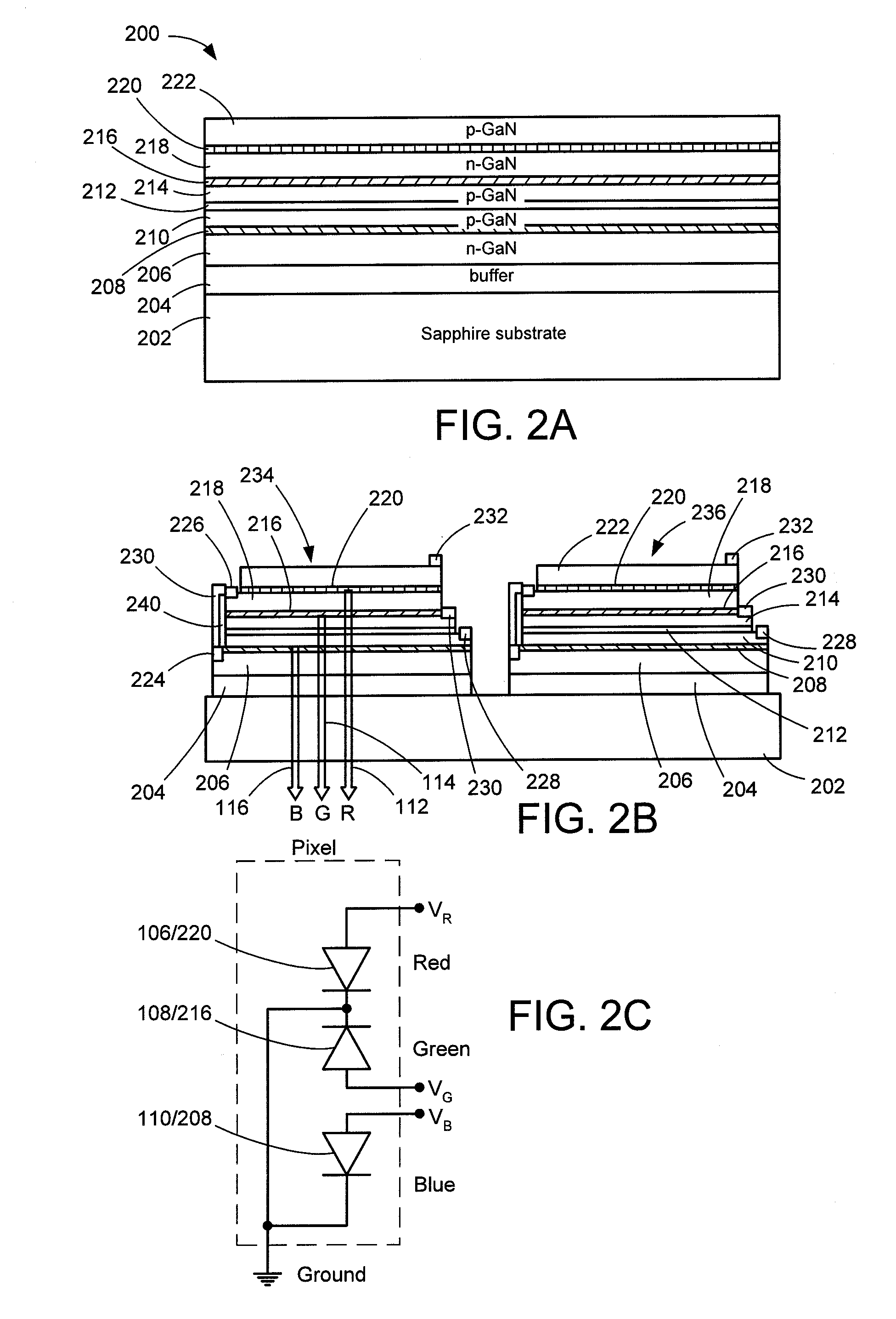
[0037]Embodiments of the present invention provide color microdisplay elements systems and methods for making those elements. More specifically, disclosed is a semiconductor micro-emitter array based microdisplays, and in particular to full-color microdisplays with each pixel containing three micro-emitters—red, green, and blue (RGB)—vertically stacked up to minimize pixel size. The microdisplay may be exclusively based on Group III-nitride semiconductors, with differing indium concentrations in three respective InGaN / GaN active regions for emitting the three RGB colors. Alternatively the microdisplay may be based on hybrid integration of InGaN based III-nitride semiconductors for blue and green emissions, and AlGaInP based (e.g., Group III-V) semiconductors for red emissions. It is possible that other III-V structures could be used instead of AlGaInP, however.

[0038]In embodiments, the hybrid integration may be based on wafer bonding, such as SiO2 based adhesive wafer bonding as des...


PUM


Abstract

Disclosed is a semiconductor micro-emitter array for use in a full-color microdisplay. Each pixel includes three vertically-stacked red, green, and blue micro-emitters which minimizes pixel size. The microdisplay may be exclusively based on Group III-nitride semiconductors, with differing indium concentrations in three respective InGaN/GaN active regions for emitting the three RGB colors. Alternatively the microdisplay may be based on hybrid integration of InGaN based III-nitride semiconductors for blue and green emissions, and AlGaInP based (e.g., Group III-V) semiconductors for red emissions.

Description

CROSS-REFERENCE TO RELATED APPLICATIONS[0001]This application claims the benefit of U.S. Provisional Application No. 60 / 975,381 filed Sep. 26, 2007, the disclosure of which is incorporated herein by reference.BACKGROUND OF THE INVENTION[0002]1. Field of the Invention[0003]The invention relates generally to the field including microdisplay devices and the methods of making them. More specifically, the invention relates to the fabrication of RGB pixels for use in microdisplays.[0004]2. Description of the Related Art[0005]Microdisplays have many military and civilian applications, for example to provide head-mounted displays, hand-held projectors, heads-up displays, and other near-to-eye applications. Microdisplays with high resolution, power efficiency, reliability, and other merits may enable various high-performance portable applications. One category of microdisplays is modulating microdisplays, such as liquid crystal or digital mirror device (DMD) based displays. These are relativ...

Claims


Application Information

Patent Timeline
Patent Type & Authority Applications(United States)
IPC IPC(8): H01L33/00H01L21/00
CPCH01L27/156H01L27/15
Inventor FAN, ZHAOYANGLI, JINGLIN, JINGYUJIANG, HONGXING
Owner III N TECH
Why Eureka
Try Eureka