
Semiconductor integrated circuit

Inactive Publication Date: 2009-03-26
RENESAS TECH CORP
View PDF3 Cites 22 Cited by
  • Summary
  • Abstract
  • Description
  • Claims
  • Application Information

AI Technical Summary

Benefits of technology

[0020]An advantageous effect obtained by a representative one of the inventions disclosed in the present application will be explained briefly as follows.
[0021]There can be provided a semiconductor integrated circuit that has made each power shutdown area appropriate.

Problems solved by technology

When, however, leak current at the turning off of a transistor is large, the effect of reducing power consumption is not enough even though the supply of the clock to the inside of the functional module kept in the standby state is stopped.
Therefore, an input gate of power shutdown-free functional module with the signal being used as an input is brought into floating, thus resulting in the occurrence of leakage current in the input gate.

Method used


Image

  • Semiconductor integrated circuit
  • Semiconductor integrated circuit
  • Semiconductor integrated circuit

Examples


Embodiment Construction

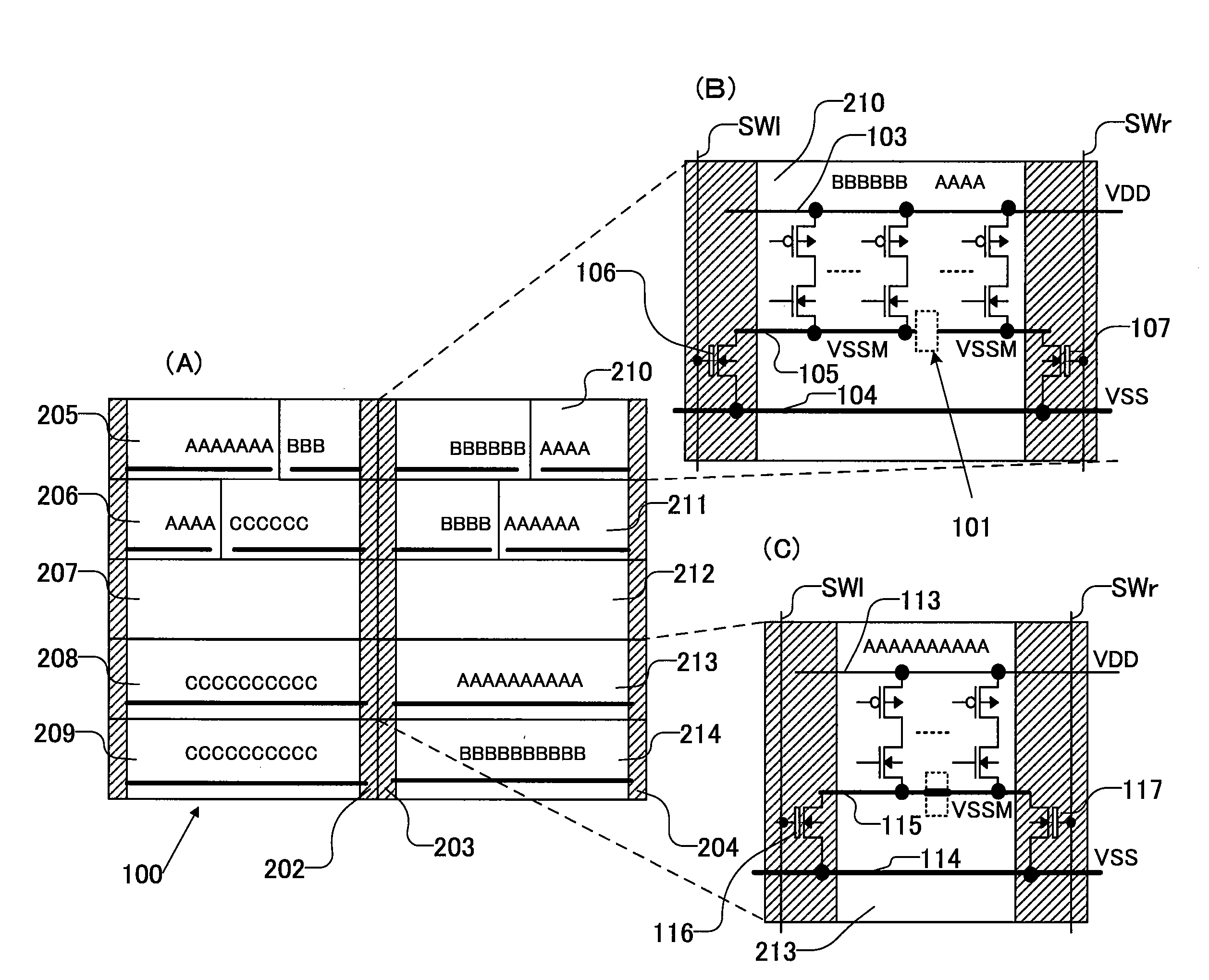
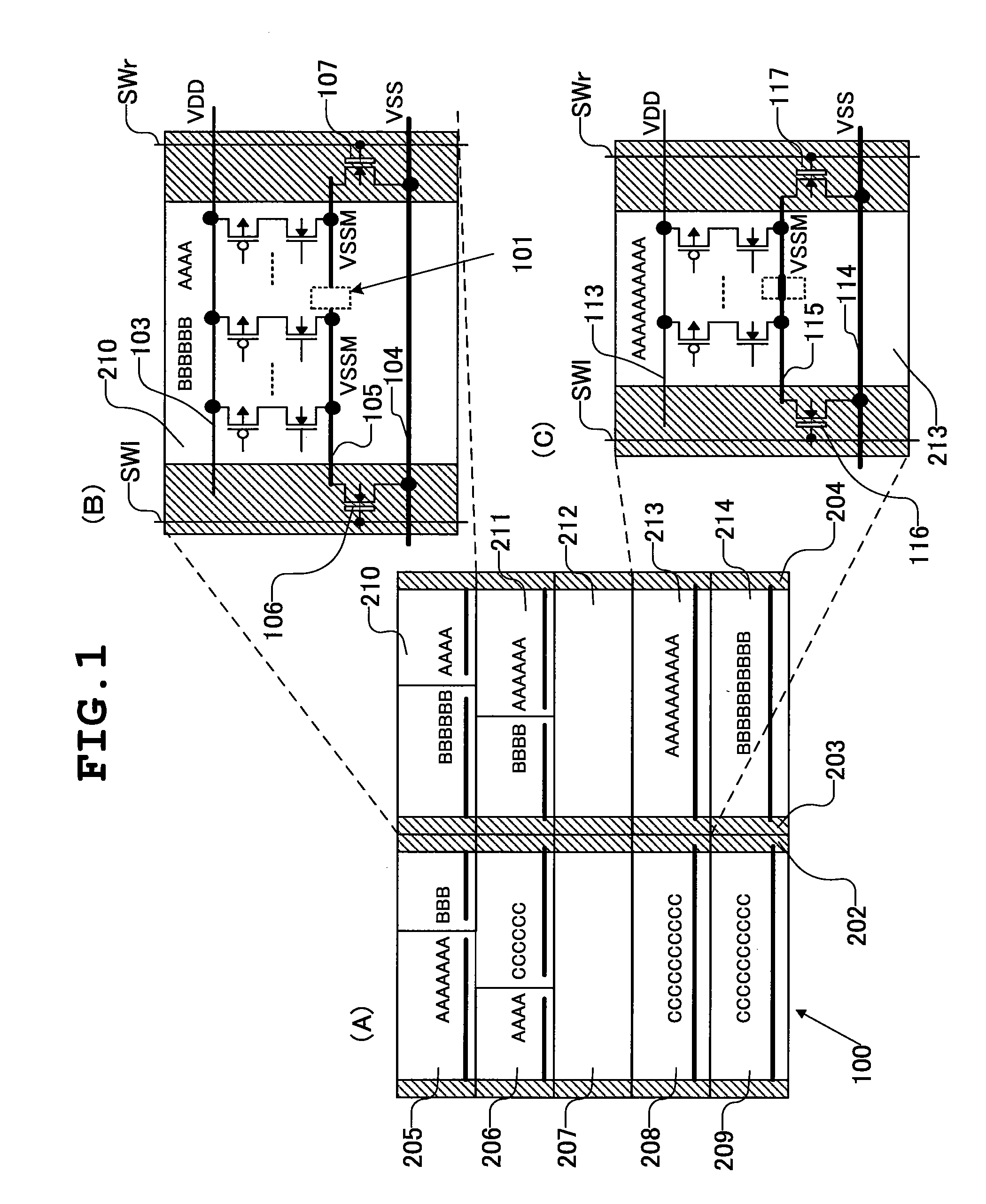
[0054]A configuration example of a semiconductor integrated circuit according to the present invention is shown in FIG. 1(A).

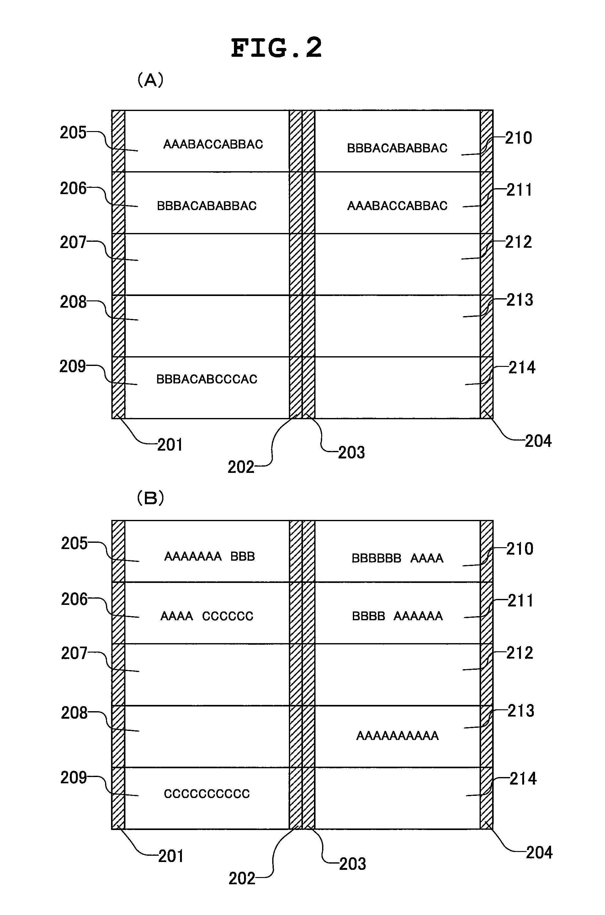
[0055]Although not restricted in particular, the semiconductor integrated circuit 100 shown in FIG. 1(A) is configured as a microcomputer formed in one semiconductor substrate such as a monocrystal silicon substrate by the known semiconductor integrated circuit manufacturing technology. The semiconductor integrated circuit 100 includes a plurality of cell areas 205 through 214, and power switch circuits 201 through 204 capable of cutting off the supply of power to the cell areas 205 through 214. The power switch circuits are respectively disposed on both sides of the cell areas 205 through 214. In the cell areas 205 through 214, A through F indicate power shutdown groups. The power shutdown groups A through F enable the cut-off of the supply of power by means of their corresponding power switch circuits 201 through 204. When different power shutdown groups are...


PUM


Abstract

The present invention aims to make each power shutdown area appropriate.Cell areas each comprising a plurality of core cells arranged therein, and power switches disposed corresponding to the respective cell areas are provided. A plurality of power shutdown areas are respectively formed in units of the core cells. In each power shutdown area, power shutdown is enabled by the power switches corresponding to the power shutdown areas. Thus, the power shutdown areas can be set finely in the core cell units, and the appropriateness of each power shutdown area is achieved. With its appropriateness, a reduction in current consumption at standby is achieved.

Description

TECHNICAL FIELD[0001]The present invention relates to a layout technology of a semiconductor integrated circuit, and particularly to a technology effective if applied to a semiconductor integrated circuit in which a number of minimum cells (hereinafter described as core cells) constituted of transistors and logic gates are coupled thereby to form functional modules having predetermined functions.BACKGROUND ART[0002]A typical method for reducing power consumption at the time when each of functional modules in a semiconductor integrated circuit is kept in a standby state, is to stop a clock supplied to the inside of each functional module. When, however, leak current at the turning off of a transistor is large, the effect of reducing power consumption is not enough even though the supply of the clock to the inside of the functional module kept in the standby state is stopped. As a semiconductor integrated circuit capable of cutting off leakage current flowing through an unused circuit...

Claims


Application Information

Patent Timeline
IPC IPC(8): H03K17/16
CPCH01L27/11803H01L27/0207
Inventor SASAKI, TOSHIOYASU, YOSHIHIKOMORI, RYOISHIBASHI, KOICHIROKANNO, YUSUKE
Owner RENESAS TECH CORP
Learn More