Synchronous Address And Data Multiplexed Mode For SRAM

a synchronous address and data multiplexing technology, applied in the field of synchronous memory system, can solve the problems of limited space on the printed circuit board, and intel® flash memory can only perform asynchronous write operations

Active Publication Date: 2009-04-02
SK HYNIX INC
View PDF12 Cites 12 Cited by
  • Summary
  • Abstract
  • Description
  • Claims
  • Application Information

AI Technical Summary

Benefits of technology

[0012]The present invention will be more fully understood in view of the following description and drawings.

Problems solved by technology

In some applications, such as cellular phones, there is a limited space for a printed circuit board (PCB).
However, this Intel® flash memory can only perform asynchronous write operations, which require the use of extra control signals (i.e., extra PCB routing wires).

Method used


Image

  • Synchronous Address And Data Multiplexed Mode For SRAM
  • Synchronous Address And Data Multiplexed Mode For SRAM
  • Synchronous Address And Data Multiplexed Mode For SRAM

Examples


Embodiment Construction

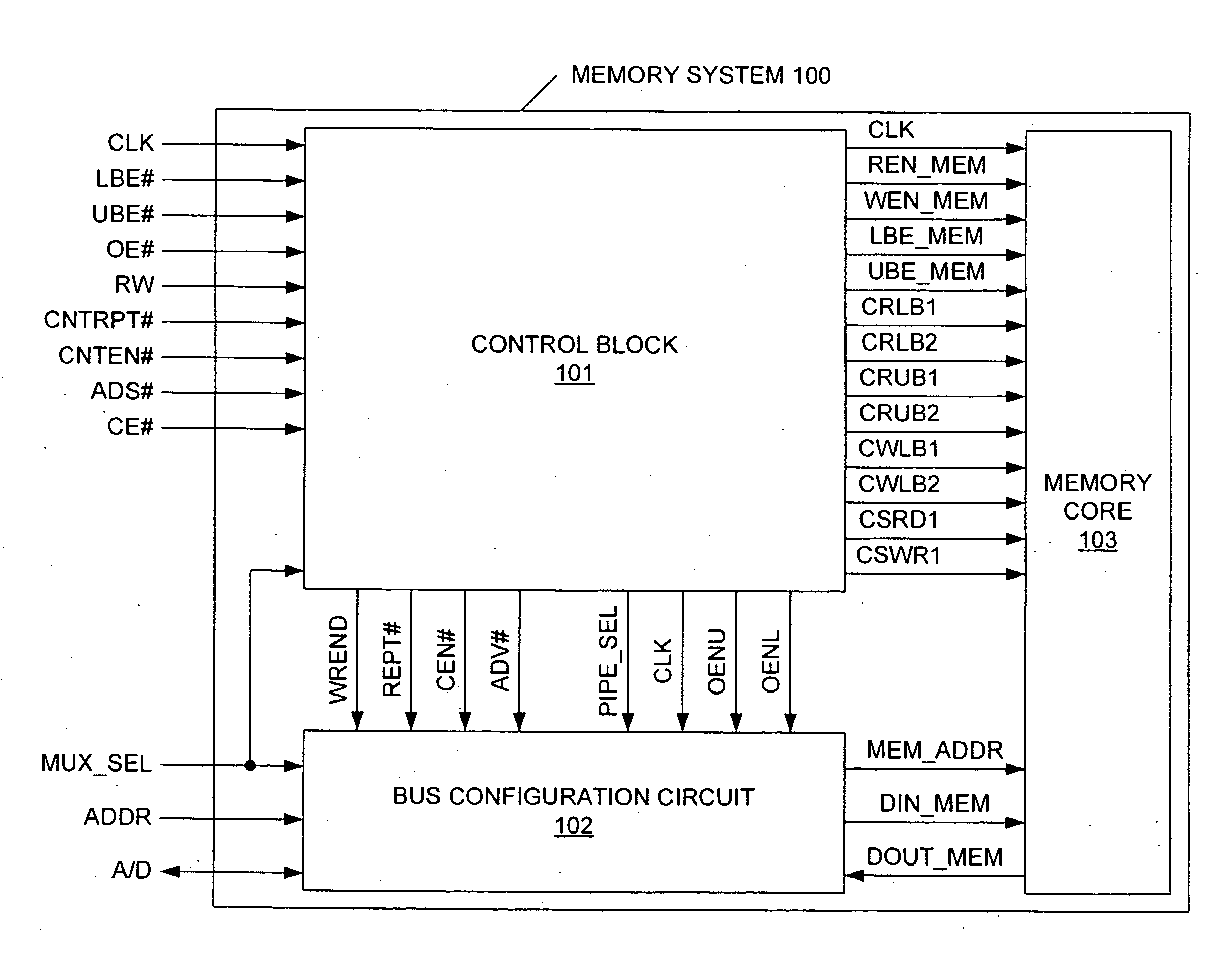
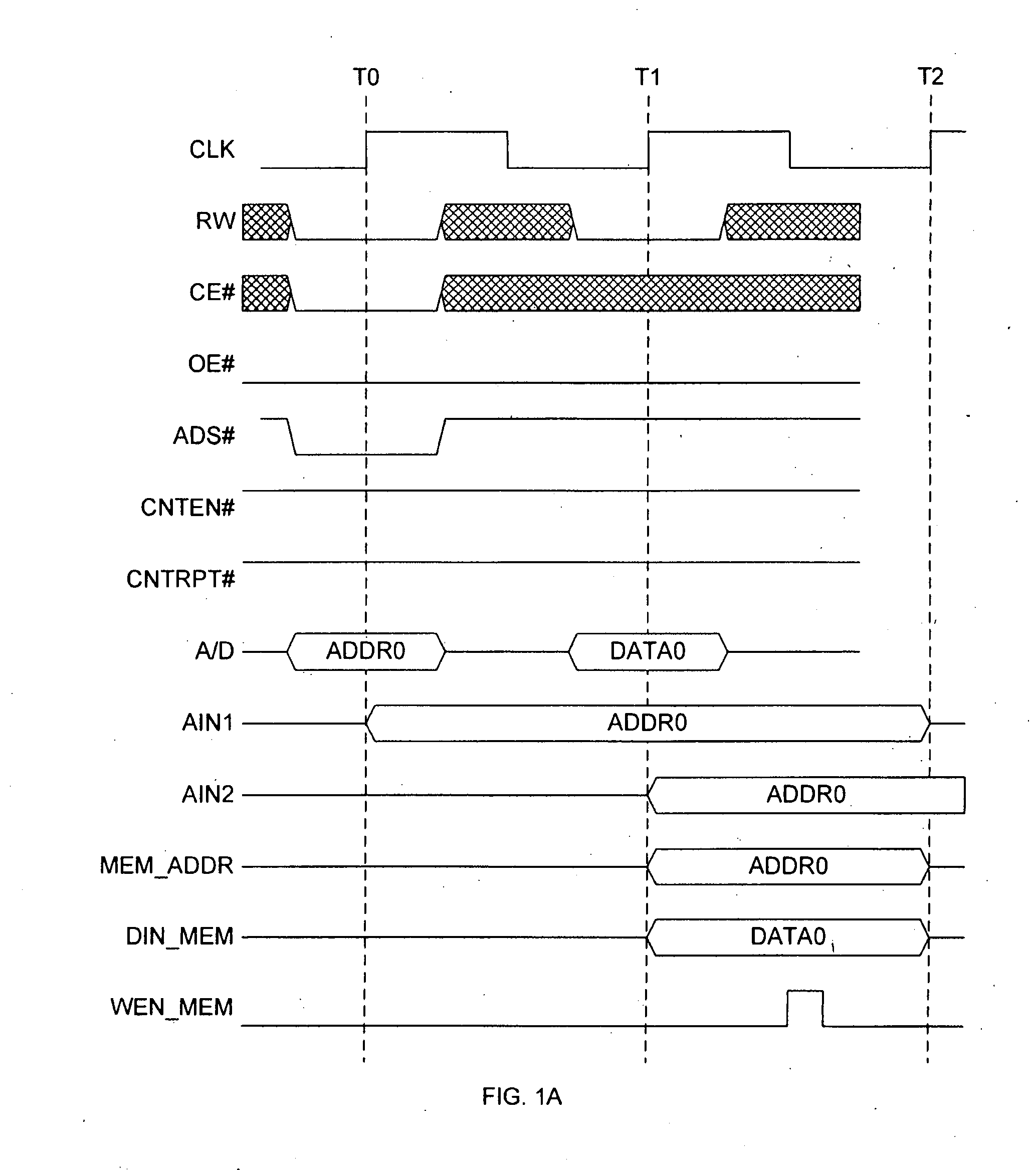
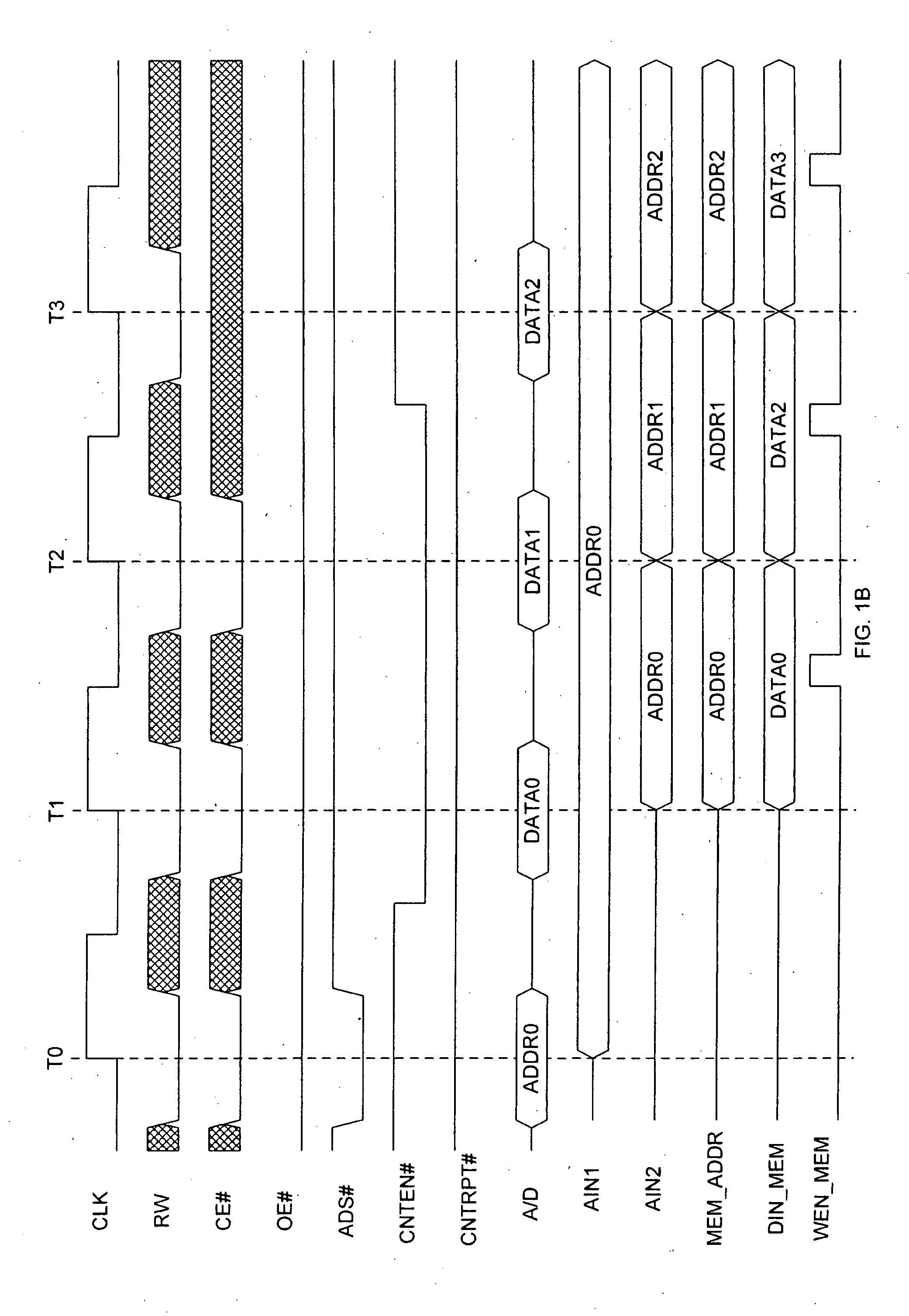
[0024]In accordance with one embodiment of the present invention, an address / data (A / D) muxed mode is added to a conventional memory system, such as that defined in IDT data sheet IDT70T3519 / 99 / 89S, entitled “High-Speed 2.5 V 256 / 128 / 64 Kx36 Synchronous Dual-port Static RAM with 3.3V or 2.5V Interface”, which is hereby incorporated by reference. The present invention provides a synchronous memory system that enables address and data signals to be transmitted on a shared set of address / data bus lines (pins) in the A / D muxed mode. The memory system of the present invention is also capable of being operated in a non-muxed mode, wherein address signals are provided on dedicated address bus lines (which are not used in the A / D muxed mode), and data signals are provided on the A / D bus lines.

[0025]As described in more detail below, operations in the A / D muxed mode are qualified by commands in order to eliminate potential bus turn around problems on the multiplexed address / data bus lines. M...


PUM


Abstract

A synchronous memory system configurable in a multiplexed or non-multiplexed mode. In the multiplexed mode, address and data are provided on a shared bus, and accesses to the memory system are qualified by memory access control signals, including an address strobe signal, a counter enable signal and a counter repeat signal. A read/write control signal is maintained for one cycle after the last valid access command to avoid bus turn-around problems. In the multiplexed mode, chip enable and output enable signals may be constantly activated, thereby simplifying associated printed circuit board design. Different ports of the synchronous memory system can be independently configured to operate in either the multiplexed or non-multiplexed mode.

Description

BACKGROUND OF THE INVENTION[0001]1. Field of the Invention[0002]The present invention relates to a synchronous memory system having a mode in which address and data signals can be multiplexed on the same set of signal lines.[0003]2. Related Art[0004]In some applications, such as cellular phones, there is a limited space for a printed circuit board (PCB). If an application uses a static random access memory (SRAM) chip that requires a 16-bit data bus and a 14-bit address bus, the associated PCB will require at least 30 corresponding routing wires to enable the SRAM chip to communicate with other chips.[0005]It would therefore be desirable to share the address bus with the data bus, thereby minimizing the number of routing wires required on the PCB. An operating mode in which address and data signals are multiplexed onto the same set of bus lines is hereinafter referred to as a address / data (A / D) muxed mode.[0006]Intel® provides a flash memory that shares an address bus with a data bu...

Claims


Application Information

Patent Timeline
Patent Type & Authority Applications(United States)
IPC IPC(8): G06F12/00
CPCG06F13/4243G11C11/413G11C7/1075
Inventor SPRINGER, CASEY
Owner SK HYNIX INC
Why Eureka
Try Eureka