CMOS image sensor having thiophene derivatives

a thiophene derivative and image sensor technology, applied in the direction of thermoelectric devices, solid-state devices, radiation control devices, etc., can solve the problems of reducing the light input to the photodiode and the sensitivity of the cmos image sensor

Active Publication Date: 2009-04-09
SAMSUNG ELECTRONICS CO LTD
View PDF7 Cites 26 Cited by
  • Summary
  • Abstract
  • Description
  • Claims
  • Application Information

AI Technical Summary

Problems solved by technology

The color filter absorbs approximately ⅔ of light incident on the photodiode, and thus, the amount of l...

Method used


Image

  • CMOS image sensor having thiophene derivatives
  • CMOS image sensor having thiophene derivatives
  • CMOS image sensor having thiophene derivatives

Examples


Embodiment Construction

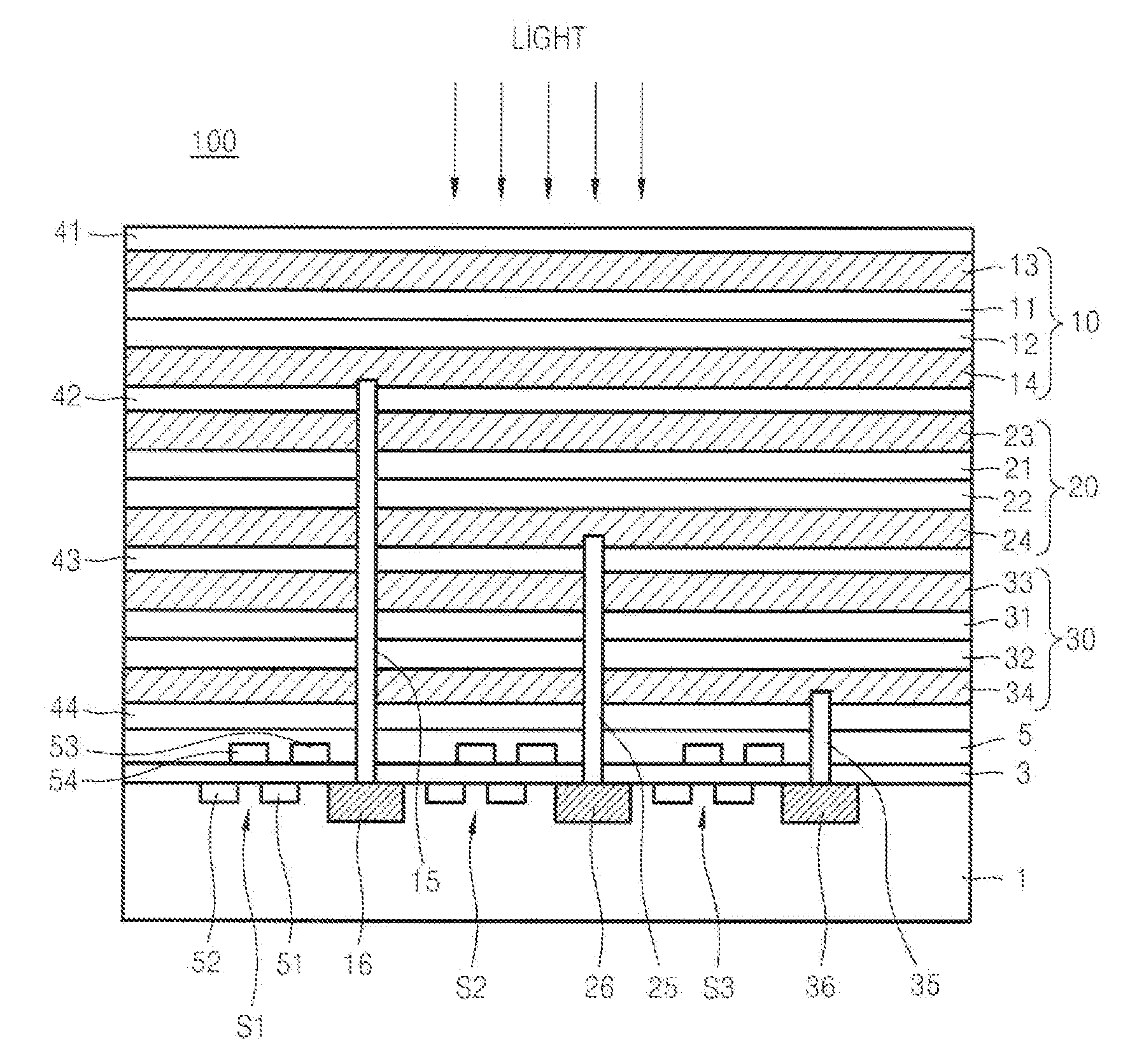
[0028]A vertically-stacked complimentary metal oxide semiconductor (CMOS) image sensor and a method of manufacturing the same according to the present invention will now be described more fully with reference to the accompanying drawings in which exemplary embodiments of the invention are shown.

[0029]FIG. 1 is a cross-sectional view of a vertical CMOS image sensor 100 having thiophene derivatives, according to an embodiment of the present invention.

[0030]Referring to FIG. 1, the vertically-stacked CMOS image sensor 100 according to the current embodiment of the present invention includes first through third photoelectric conversion units 10, 20, and 30 vertically and sequentially stacked on a semiconductor substrate 1. A transparent insulating layer 41 is formed on an upper surface of the first photoelectric conversion unit 10, a transparent insulating layer 44 is formed on a lower surface of the third photoelectric conversion unit 30, and transparent insulating layers 42 and 43 are...


PUM

PropertyMeasurementUnit
Depthaaaaaaaaaa

Abstract

Provided is a CMOS image sensor that uses thiophene derivatives. The CMOS image sensor includes first through third photoelectric conversion units vertically and sequentially stacked on a semiconductor substrate. The first photoelectric conversion unit detects blue light and comprises a first electrode, a second electrode, and a p-type thiophene derivative layer between the first electrode and the second electrode.

Description

CROSS-REFERENCE TO RELATED PATENT APPLICATION[0001]This application claims the benefit of Korean Patent Application No. 10-2007-0100944, filed on Oct. 8, 2007, in the Korean Intellectual Property Office, the disclosure of which is incorporated herein in its entirety by reference.BACKGROUND OF THE INVENTION[0002]1. Field of the Invention[0003]The present invention relates to a vertical CMOS image sensor, and more particularly, to a CMOS image sensor that uses blue photoelectric conversion characteristics of a p-n junction body having an n-characteristic and a p-characteristic of thiophene derivatives.[0004]2. Description of the Related Art[0005]An image sensor is a photoelectric transducer that detects light and transforms the detected light into an electric signal. A conventional image sensor includes a plurality of unit pixels arranged in arrays on a semiconductor substrate. Each of the unit pixels includes a photodiode and transistors. The photodiode generates and stores optical c...

Claims


Application Information

Patent Timeline
IPC IPC(8): H01L51/42
CPCH01L27/14647H01L27/307H01L51/0085H01L51/0068H01L51/0071H01L51/0036H10K39/32H10K85/113H10K85/655H10K85/657H10K85/342H01L27/146
Inventor KIM, KYU-SIKPARK, SANG-CHEOLPARK, YOUNG-JUNKWON, O-HYUNNAM, JUNG-GYUJO, HYE-SUK
Owner SAMSUNG ELECTRONICS CO LTD
Why Eureka
Try Eureka