Driving circuit apparatus

a circuit apparatus and driving circuit technology, applied in the direction of electric digital data processing, instruments, computing, etc., can solve the problems of increasing the number of data lines achieve the effects of reducing the chip size of the source driver, reducing the number of data lines, and maintaining image quality

Inactive Publication Date: 2009-04-16
LAPIS SEMICON CO LTD
View PDF10 Cites 12 Cited by
  • Summary
  • Abstract
  • Description
  • Claims
  • Application Information

AI Technical Summary

Benefits of technology

[0018]As described above, according to the present invention, it is possible to provide a driving circuit apparatus which is capable of achieving reduction in chip size of a source driver by reducing the number of data lines within the source driver, while maintaining image quality even when an image data is configured by multiple bits.

Problems solved by technology

However, if image data is configured by multiple bits (multi-gradation) for either an analog gamma correction or a digital gamma correction, this leads to an increase in the number of data lines of a source driver.

Method used


Image

  • Driving circuit apparatus
  • Driving circuit apparatus
  • Driving circuit apparatus

Examples


first embodiment

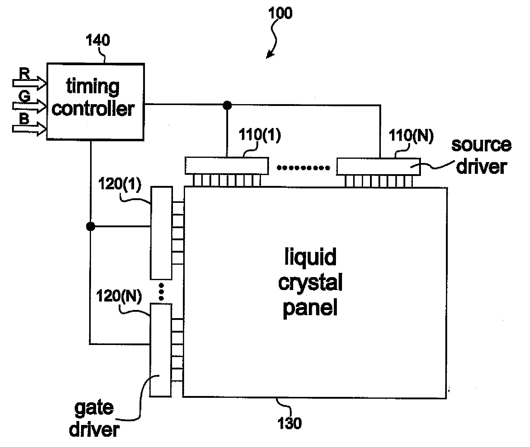
[0028]FIG. 1 is a configurational view of a liquid crystal display 100 according to the present invention. Liquid crystal display (LCD) 100 includes a timing controller 140, source drivers 110(1), . . . , 110(N) (N is an integer of more than 1), gate drivers 120(1), . . . , 120(N), and a liquid crystal panel 130. Hereinafter, the source drivers 110(1), . . . , 110(N) may be sometimes generally called a source driver 110 as a single unit, and similarly the gate drivers 120(1), . . . , 120(N) may be sometimes generally called a gate driver 120. The timing controller 140 is connected to the source drivers 110(1), . . . , 110(N) and the gate drivers 120(1), . . . , 120(N). The source drivers 110(1), . . . , 110(N) and the gate drivers 120(1), . . . , 120(N) are connected to the liquid crystal panel 130.

[0029]In a display method of the LCD 100, the timing controller 140 receives image data including an RGB (Red-Green-Blue) signal output from a graphic processor or the like, transmits a l...

second embodiment

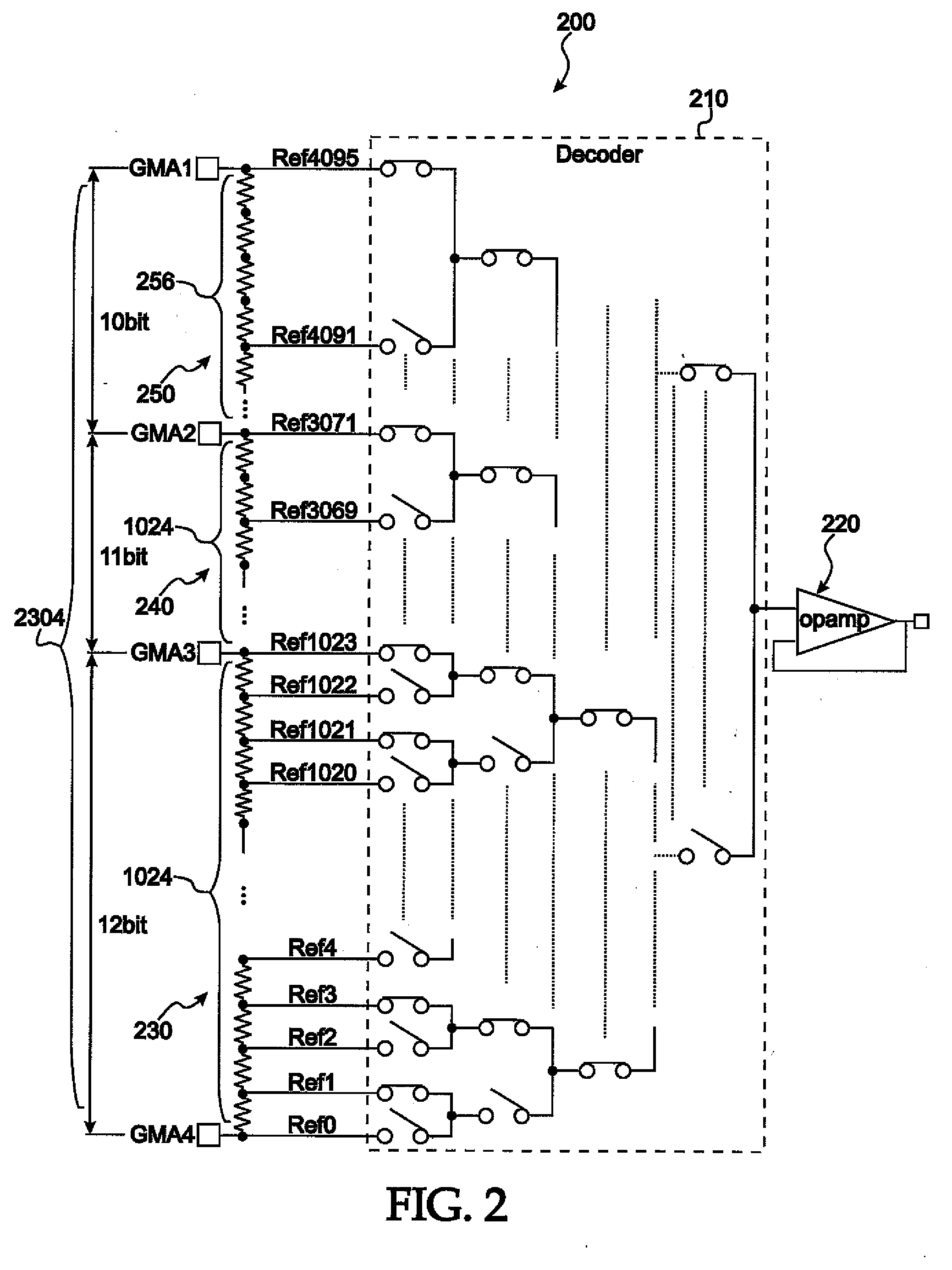
[0043]FIG. 6 is a second configurational view 600 of a source driver 110 according to the present invention. As shown in the second configurational view 600, the source driver 110 includes GMA1, GMA2, GMA3, GMA4, data lines (plural input data lines), a decoder 610, and an operational amplifier (hereinafter abbreviated as OP Amp) 620. The data lines include 2048 input data lines Ref0 to Ref4095 (representing 2048 gray scales) (excluding 2047 unused input data lines having no wiring), and the OP Amp 620 is used as a voltage follower circuit.

[0044]In addition, as shown in the second configurational view 600 in FIG. 6, a range between GMA3 and GMA4 with fineness of 12 bits is defined as a fourth region 630, a range between GMA2 and GMA3 with fineness of 11 bits is defined as a fifth region 640, and a range between GMA1 and GMA2 with fineness of 10 bits is defined as a sixth region 650, in all of which regions resistive elements are connected in series.

[0045]In more detail, 1024 input si...


PUM


Abstract

A driving circuit that reduces chip size of a source driver while maintaining image quality when image data is configured by multiple bits. The source driver provided in connection with a timing controller that converts image data into color data. The source driver displays an image by controlling pixel density of a liquid crystal panel. The source driver is divided into plural regions in units of pseudo linear elements to perform a gamma correcting operation based on a gamma characteristic. In the source driver a GMA voltage for each region is divided by resistive elements arranged between input signal lines. With respect to variation of plural divided GMA voltages, variation of the maximum high density region becomes coarser than variation of the maximum low density region in compliance with visual sensitivity of the density, thus reducing the number of input data lines of the source driver.

Description

[0001]The present application claims priority under 35 U.S.C. 119 to Japanese patent application serial number 2007 / 269113, filed on Oct. 16, 2007, which is hereby incorporated by reference in its entirety for all purposes.BACKGROUND OF THE INVENTION[0002]1. Field of the Invention[0003]The present invention relates to a driving circuit apparatus, and more particularly to reducing chip size of a source driver in a liquid crystal driver circuit.[0004]2. Description of the Related Art[0005]In general, in a display method for a liquid crystal display (LCD), a timing controller receives image data output from a graphic processor or the like, transmits a line select signal to a gate driver, and outputs color data to a source driver. The source driver divides a GMA (Gamma) voltage, which represents a voltage value of a gray scale for a color, by resistors; provides a voltage depending on color data to a liquid crystal panel; and displays an image at lines selected by the gate driver from t...

Claims


Application Information

Patent Timeline
Patent Type & Authority Applications(United States)
IPC IPC(8): G09G5/02G09G5/10
CPCG09G3/3685G09G2320/0285G09G2320/0276G09G3/3696
Inventor KINOSHITA, HIROYUKI
Owner LAPIS SEMICON CO LTD
Why Eureka
Try Eureka