Pixel Sensing Circuit and Pixel Sensing Method

a pixel sensing circuit and pixel sensing technology, applied in the direction of instruments, static indicating devices, etc., can solve the problems of increasing the chip size and manufacture cost degrading the image quality of the oled display device, etc., to reduce the size of the source driver ic and the size of the pixel sensing circuit.

Active Publication Date: 2022-06-09
LX SEMICON CO LTD
View PDF0 Cites 0 Cited by
  • Summary
  • Abstract
  • Description
  • Claims
  • Application Information

AI Technical Summary

Benefits of technology

[0014]As described above, according to an embodiment, since a current integrator circuit is shared in a pixel sensing circuit, it is possible to reduce the size of the pixel sensing circuit. Further, it is also possible to reduce the size of a source driver IC including the pixel sensing circuit and manufacture costs thereof.

Problems solved by technology

When the electrical characteristics of the pixels are different, a brightness difference occurs even between pixels supplied with the same data voltage, thus degrading the image quality of the OLED display device.
Accordingly, an area occupied by the pixel sensing circuit in the source driver IC is increased, thus increasing the chip size and manufacture costs of the source driver IC.

Method used


Image

  • Pixel Sensing Circuit and Pixel Sensing Method
  • Pixel Sensing Circuit and Pixel Sensing Method
  • Pixel Sensing Circuit and Pixel Sensing Method

Examples


Embodiment Construction

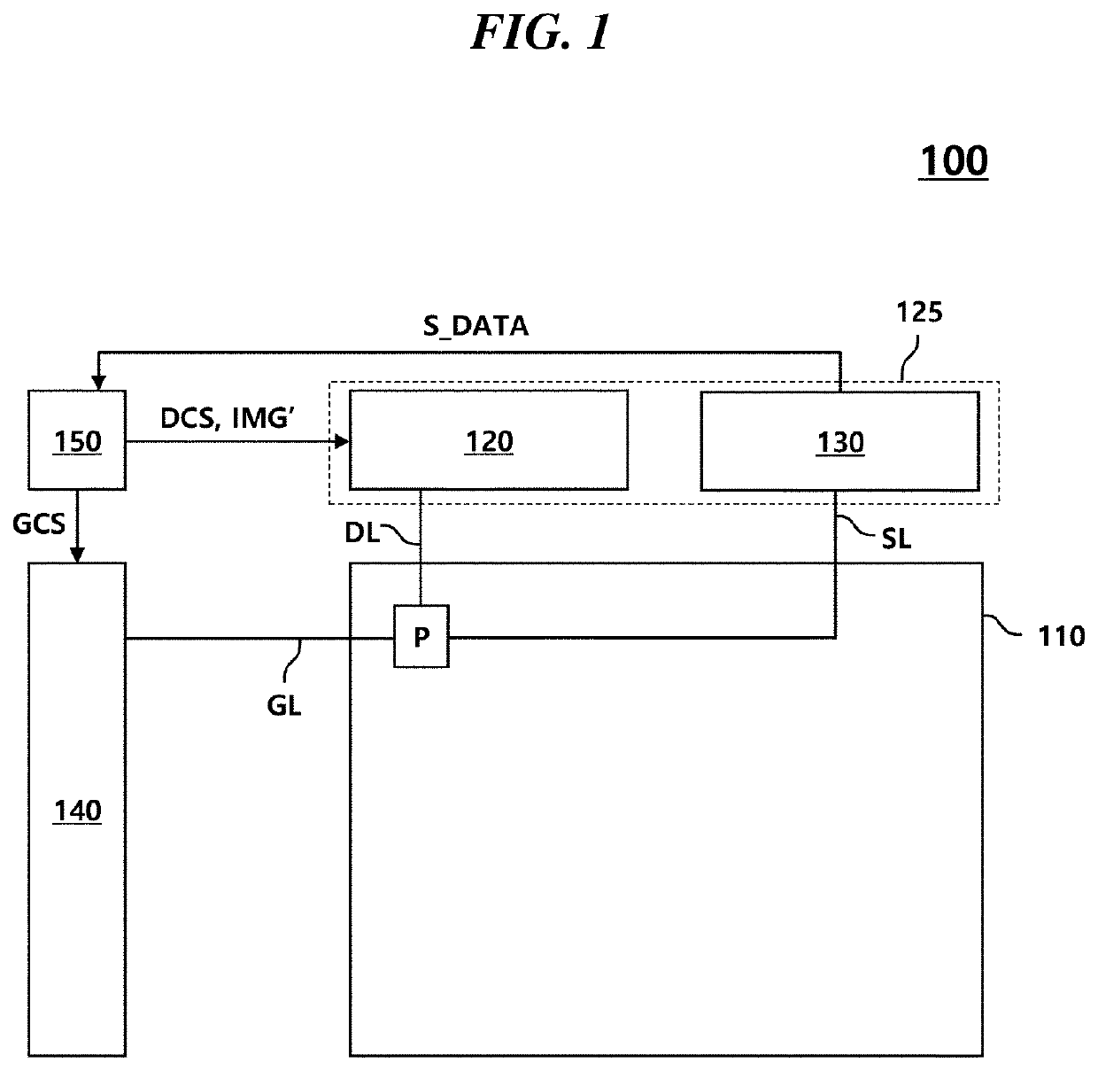
[0026]FIG. 1 illustrates the configuration of a general display device.

[0027]Referring to FIG. 1, the general display device 100 may include a display panel 110 and a panel driving device 120, 130, 140, and 150 to drive the display panel 110.

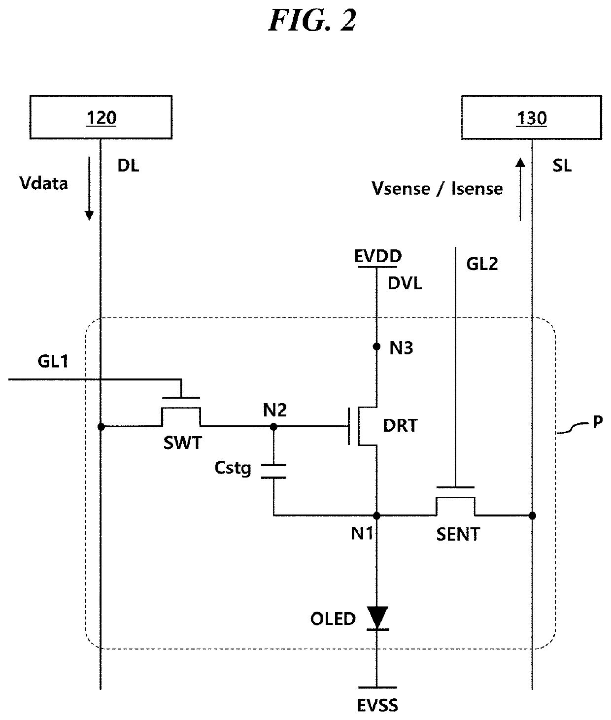
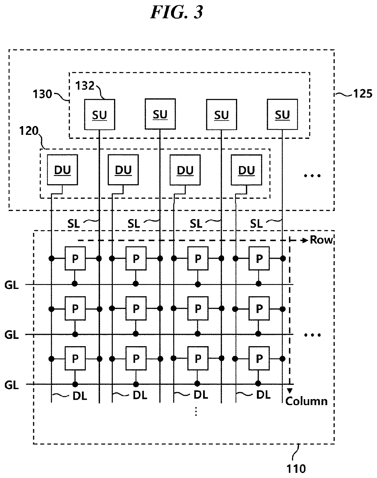
[0028]On the display panel 110, a plurality of data lines DL, a plurality of gate lines GL, and a plurality of sensing lines SL may be disposed, and a plurality of pixels P may be disposed. Here, the plurality of pixels P may be disposed in the form of a matrix including a plurality of rows and a plurality of columns as illustrated in FIG. 3.

[0029]Devices 120, 130, 140, and 150 to drive at least one component included in the display panel 110 may be referred to as the panel driving device. For example, a data driving circuit 120, a pixel sensing circuit 130, a gate driving circuit 140, a data processing circuit 150, and the like may be referred to as the panel driving device.

[0030]Each of the devices 120, 130, 140, and 150 may be referred to as ...


PUM


Abstract

An embodiment relates to a pixel sensing circuit and a pixel sensing method and, more particularly, to a pixel sensing circuit and a pixel sensing method for reducing the size of a source driver IC by sharing some components in a pixel sensing circuit and for sensing a pixel using a pixel sensing circuit in which some components are shared.

Description

CROSS-REFERENCE TO RELATED APPLICATIONS[0001]This application claims priority from Republic of Korea Patent Application No. 10-2020-0167559, filed on Dec. 3, 2020, which is hereby incorporated by reference for all purposes as if fully set forth herein.BACKGROUND1. Field of Technology[0002]The present embodiment relates to a pixel sensing circuit and a pixel sensing method.2. Description of the Prior Art[0003]Generally, an organic light-emitting diode (OLED) display device is a display device that displays a desired image by individually supplying data voltages according to image information to OLED pixels disposed in a matrix form to thereby control the pixels.[0004]A panel applied to the OLED display device, that is, a display panel in which OLED pixels are disposed, has an increasing range of applications due to lightness, slimness, and low-power driving.[0005]Each pixel includes an organic light-emitting diode (OLED), a driving thin-film transistor (TFT), and the like. As the dri...

Claims


Application Information

Patent Timeline
Patent Type & Authority Applications(United States)
IPC IPC(8): G09G3/3283
CPCG09G3/3283G09G2310/061G09G2330/12G09G2300/0842G09G2310/08G09G3/006G09G3/3233G09G2320/0295G09G3/3275G09G2320/0233
Inventor KIM, YOUNG BOKKIM, WONSHIN, YOUNG HO
Owner LX SEMICON CO LTD
Why Eureka
Try Eureka