Semiconductor device and manufacturing method thereof

a technology of semiconductors and semiconductors, applied in the direction of semiconductor devices, electrical devices, transistors, etc., can solve the problem that the carrier mobility in the channel of finfet has not been improved

Active Publication Date: 2009-04-23
KIOXIA CORP
View PDF14 Cites 47 Cited by
  • Summary
  • Abstract
  • Description
  • Claims
  • Application Information

AI Technical Summary

Problems solved by technology

However, in the techniques of Japanese Patent Application Laid-open No. 2006-351975 and WO2004 / 090992, because stress is applied to a direction perpendicular to the height direction of the fins, this has not been effective to improve carrier mobility in the channel of the FinFET.

Method used


Image

  • Semiconductor device and manufacturing method thereof
  • Semiconductor device and manufacturing method thereof
  • Semiconductor device and manufacturing method thereof

Examples


first embodiment

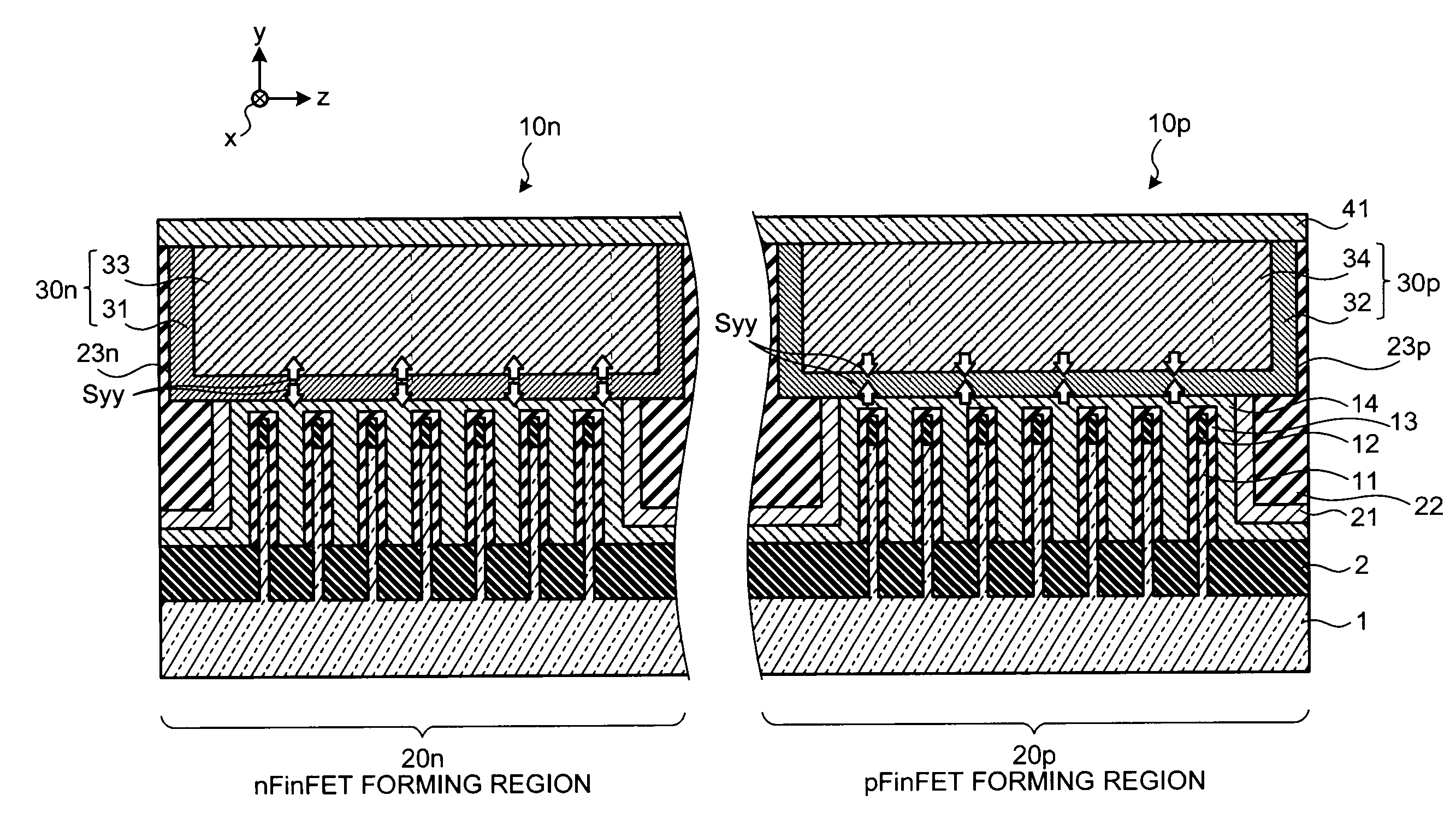
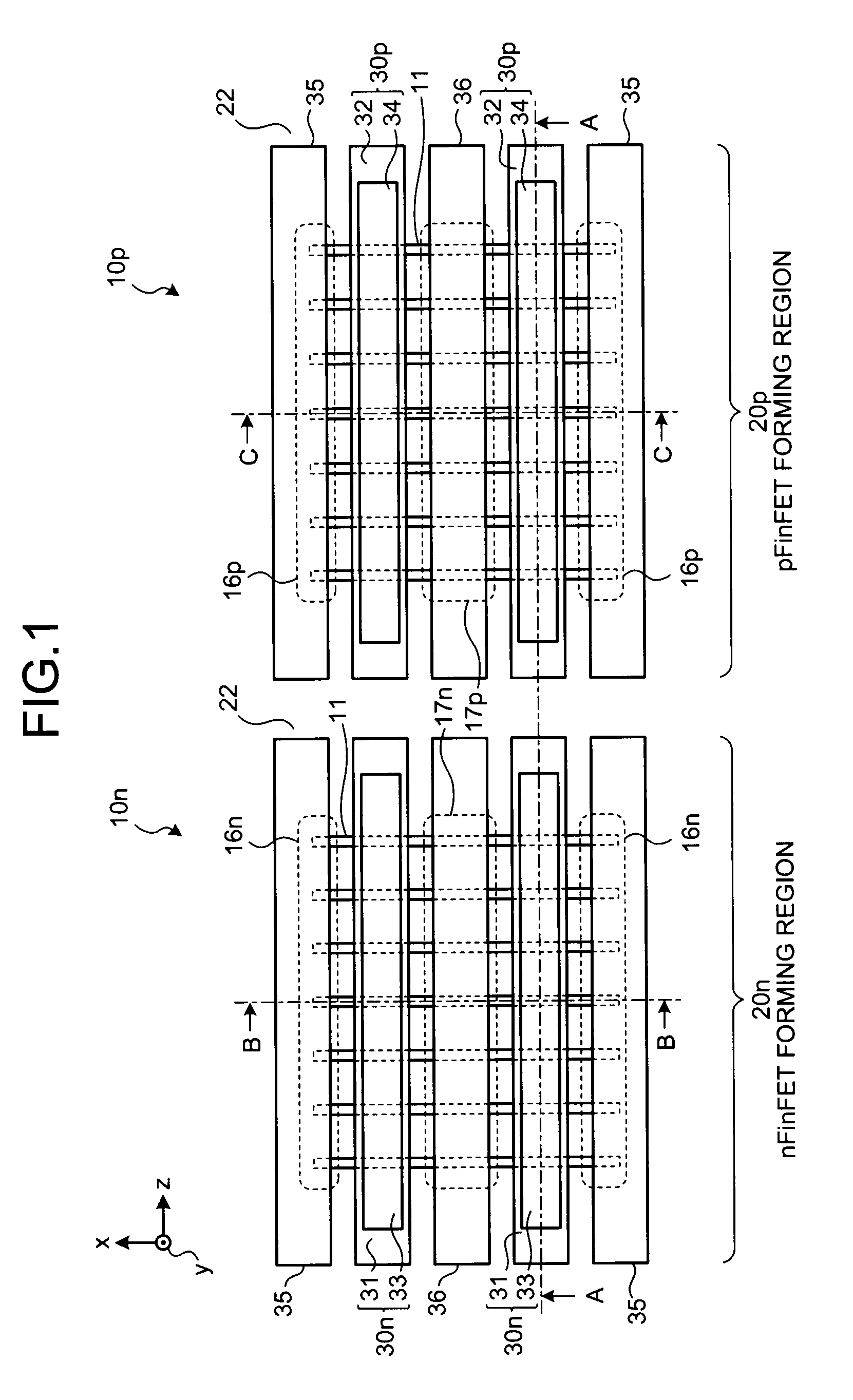
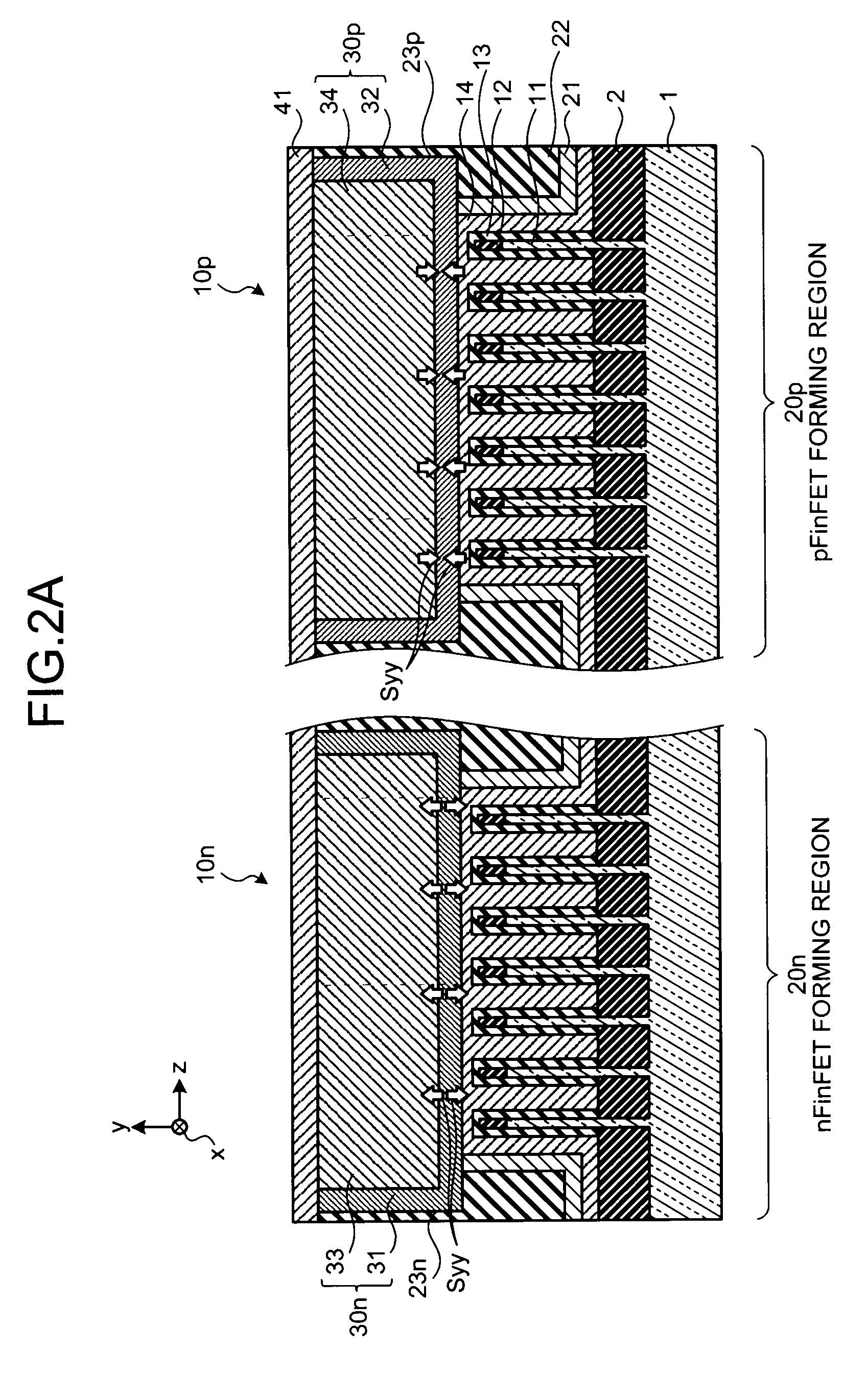
[0022]As explained above, in the first embodiment, the gate plugs 30n and 30p having lamination structures of the stress application layers 31 and 32, and the plug layers 33 and 34 are provided on the gate electrode 14. Therefore, compressive stress (in the case of the nFinFET 10n) or tensile stress (in the case of the pFinFET 10p) corresponding to a difference between a first difference and a second difference, wherein the first difference is a difference between the linear expansion coefficients at the temperature of forming the stress application layers 31 and 32 and the room temperature, and the second difference is a difference between the linear expansion coefficients at the temperature of forming the materials constituting the fins 11 and the room temperature, can be applied from the height direction (the y-axis direction) of the fins 11. In addition to this, the plug layers 33 and 34 having larger Young's modulus than that of the material constituting the fins 11 can play th...

second embodiment

[0038]In the second embodiment, in the case of the nFinFET, the stress application layer 61 is also configured by a material of which a difference between linear expansion coefficients at a temperature of forming the stress application layer 61 and the room temperature is smaller than a difference between linear expansion coefficients of a material constituting the fins 11 at a temperature of forming the stress application layer 61 and the room temperature.

[0039]In the case of the pFinFET, the stress application layer 61 is configured by a material of which a difference between linear expansion coefficients at a temperature of forming the stress application layer 61 and the room temperature is larger than a difference between linear expansion coefficients of a material constituting the fins 11 at a temperature of forming the stress application layer 61 and the room temperature.

[0040]Preferably, the plug layer 62 constituting the gate plugs 30n and 30p is formed by a material having ...

third embodiment

[0053]In the third embodiment, the polycrystalline silicon film 63 is formed on the gate electrode 14. The gate plug 30n (the plug layer 64) is formed by a metal material on this polycrystalline silicon film 63. The formed result is heat treated to silicify only the upper part of the gate electrode 14 of the polycrystalline silicon film 63, thereby forming the silicide film 65 having expanded volume. As a result, compressive stress can be applied to the fins 11 in the y-axis direction. Therefore, carrier mobility in the channel can be improved from that in the conventional nFinFET structure.

[0054]While in the above explanations, a multi-fin structure of collectively extracting current flowing through between the source and the drain obtained by plural fins 11 is explained, the embodiments can be also similarly applied to a FinFET of a single-fin structure in which one fin 11 operates as one FET. While the FinFET described above has a double-gate structure, the embodiments can be als...


PUM


Abstract

A semiconductor device according to an embodiment of the present invention comprises: a semiconductor substrate; a first field-effect transistor formed on the semiconductor substrate, and including a fin constituted by a semiconductor layer having source and drain regions via a channel region in an extending direction, and a gate electrode formed on the channel region via an insulating film; a stress application layer formed on a top surface of the gate electrode, and formed by a conductive material of which a difference between linear expansion coefficients at a temperature of forming a stress application layer and a room temperature is different from a difference between linear expansion coefficients of the fin at the temperature of forming the stress application layer and the room temperature, and a plug layer formed on the stress application layer and above the fin, and made of a conductive material having larger Young's modulus than that of the fin.

Description

CROSS-REFERENCE TO RELATED APPLICATIONS[0001]This application is based upon and claims the benefit of priority from the prior Japanese Patent Application No. 2007-274118, filed on Oct. 22, 2007; the entire contents of which are incorporated herein by reference.BACKGROUND OF THE INVENTION[0002]In a field-effect transistor using a fin structure for a channel (hereinafter, “FinFET”), a technique of applying stress to the channel has been known as a method of improving carrier mobility in the channel. For example, in Japanese Patent Application Laid-open No. 2006-351975, an insulating film covers between fins laid out in parallel and the upper part of the fins, to apply compressive stress to a direction perpendicular to a height direction of the fins, thereby improving current driving force, by utilizing a phenomenon that an insulating film works in a direction to contract. In International publication WO 2004 / 090992, a gate electrode is formed on an upper surface and on a side surface ...

Claims


Application Information

Patent Timeline
Patent Type & Authority Applications(United States)
IPC IPC(8): H01L27/088H01L21/8234
CPCH01L21/823807H01L21/823821H01L29/785H01L29/66795H01L29/7845H01L21/823828
Inventor NAGATOMO, KOJI
Owner KIOXIA CORP
Why Eureka
Try Eureka