Memory element and display device

Active Publication Date: 2009-04-23
JAPAN DISPLAY WEST
View PDF6 Cites 29 Cited by
  • Summary
  • Abstract
  • Description
  • Claims
  • Application Information

AI Technical Summary

Benefits of technology

[0013]According to the embodiments of the present invention, the memory element includes at least one dual-gate thin film transistor and one capacitor. Depending on the case, a switch formed of a thin film transistor is added thereto. Even in this case, the memory element can be formed by total two thin film transistors and one capacitor. Thus, the memory element has a greatly-simplified circuit configuration and a decreased size compared with a related-art SRAM. A plurality of memory elements thus miniaturized can easily be incorporated into a pixel, and thus a memory with a multi-bit configuration can be incorporated in the pixel with small area. Thus, it is possible to realize an active-matrix d

Problems solved by technology

In the driving of the panel of the active-matrix display device, most of the power consumption is due to the charging and discharging of the data lines.
However, it is well known that decreasing the field frequency to a value in the range of 30 to 60 Hz or lower causes flicker on the screen and thus deteriorates the display characteristics.
Because the area of the pixel aperture that allows the passage of a light beam from a backlight necessary for displaying is decreased, a bright screen cannot be obtained.
Thus, in the case of incorporating a related-art memory

Method used


Image

  • Memory element and display device
  • Memory element and display device
  • Memory element and display device

Examples


Example

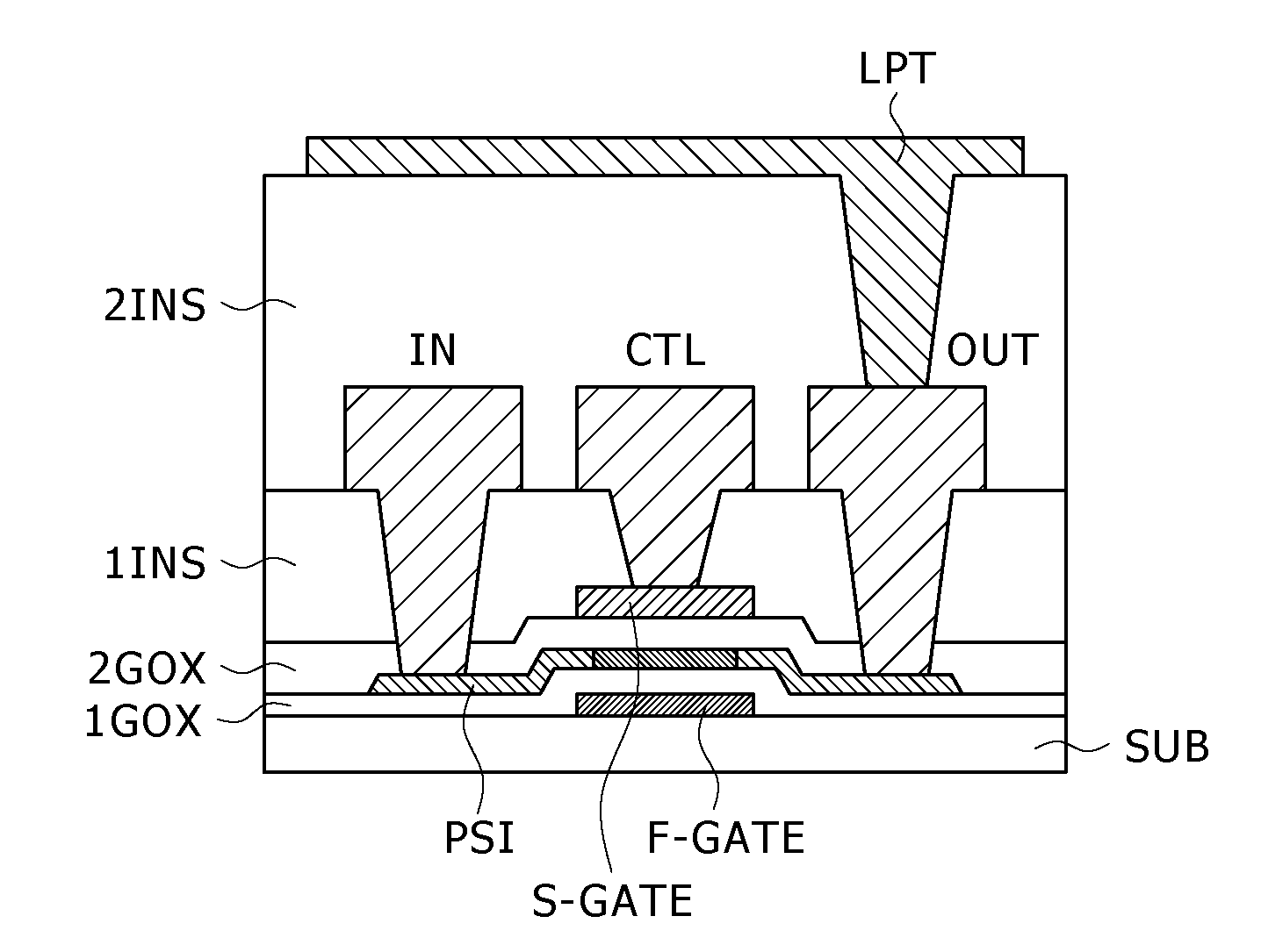
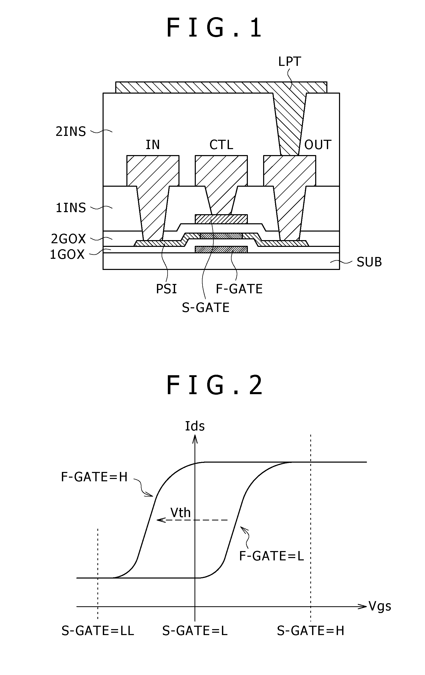
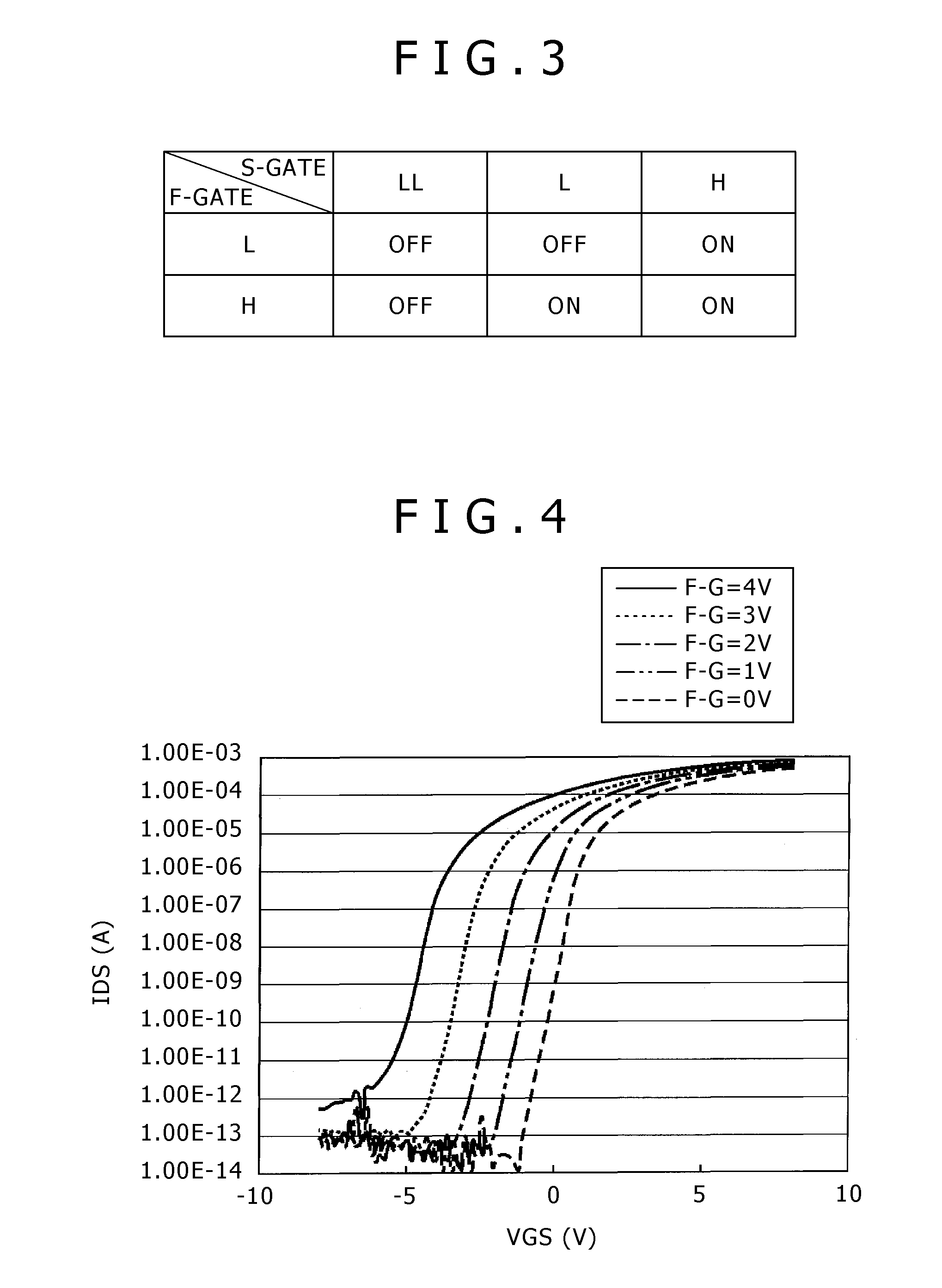
[0032]Embodiments of the present invention will be described in detail below with reference to the accompanying drawings. FIG. 1 is a schematic sectional view showing the structure of a memory element according to an embodiment of the present invention. The memory element according to the embodiment of the present invention is basically composed of a thin film transistor and a capacitor, and is formed over a substrate SUB. The thin film transistor has a semiconductor thin film PSI composed of polycrystalline silicon or the like, and a pair of gate electrodes F-GATE and S-GATE that vertically sandwich the semiconductor thin film PSI with the intermediary of insulating films 1GOX and 2GOX therebetween. The capacitor is connected to the first gate electrode F-GATE of the pair of gate electrodes, although not shown in the drawing. This capacitor can be obtained as follows. Specifically, the same conductive layer as the first gate electrode F-GATE is used as the first electrode of the ca...


PUM


Abstract

The present invention provides a memory element includes a thin film transistor configured to have a semiconductor thin film and a pair of gate electrodes that vertically sandwich the semiconductor thin film with intermediary of insulating films therebetween, and a capacitor configured to be connected to a first gate electrode of the pair of gate electrodes, wherein data is stored in the capacitor connected to the first gate electrode, and data stored in the capacitor is read out by controlling a second gate electrode of the pair of gate electrodes.

Description

CROSS REFERENCES TO RELATED APPLICATIONS[0001]The present invention contains subject matter related to Japanese Patent Application JP 2007-270119, filed in the Japan Patent Office on Oct. 17, 2007, the entire contents of which being incorporated herein by reference.BACKGROUND OF THE INVENTION[0002]1. Field of the Invention[0003]The present invention relates to memory elements. Specifically, the present invention relates to a memory element suitable for pixel driving of an active-matrix display device. Furthermore, the present invention relates to an active-matrix display device for which such a memory element is formed in each pixel.[0004]2. Description of Related Art[0005]An active-matrix liquid crystal display device includes gate lines on rows, data lines on columns, and pixels disposed at the intersections of the gate lines and the data lines. In each pixel, an electro-optical element typified by a liquid crystal cell and an active element, such as a thin film transistor, for dr...

Claims


Application Information

Patent Timeline
IPC IPC(8): G09G3/20G11C11/24G11C11/34G11C7/00
CPCG09G2300/0842G09G3/3659G02F1/13G02F1/133G02F1/136
Inventor TAKATOKU, MAKOTO
Owner JAPAN DISPLAY WEST
Why Eureka
Try Eureka