Electro-optical device

Active Publication Date: 2009-04-23
JAPAN DISPLAY INC
View PDF19 Cites 154 Cited by
  • Summary
  • Abstract
  • Description
  • Claims
  • Application Information

AI Technical Summary

Benefits of technology

[0008]An advantage of some aspects of the invention is that it provides an electro-optical device in which a driving circuit for signal lines can be disposed along an irregular part in a c

Problems solved by technology

Accordingly, there is a problem that the size of the electro-optical device becomes large, relative to the size of the pixel area.
As a result, when an image is displayed in the pixel area 10b, distinctive differe

Method used


Image

  • Electro-optical device
  • Electro-optical device
  • Electro-optical device

Examples


embodiment 1

Overall Configuration

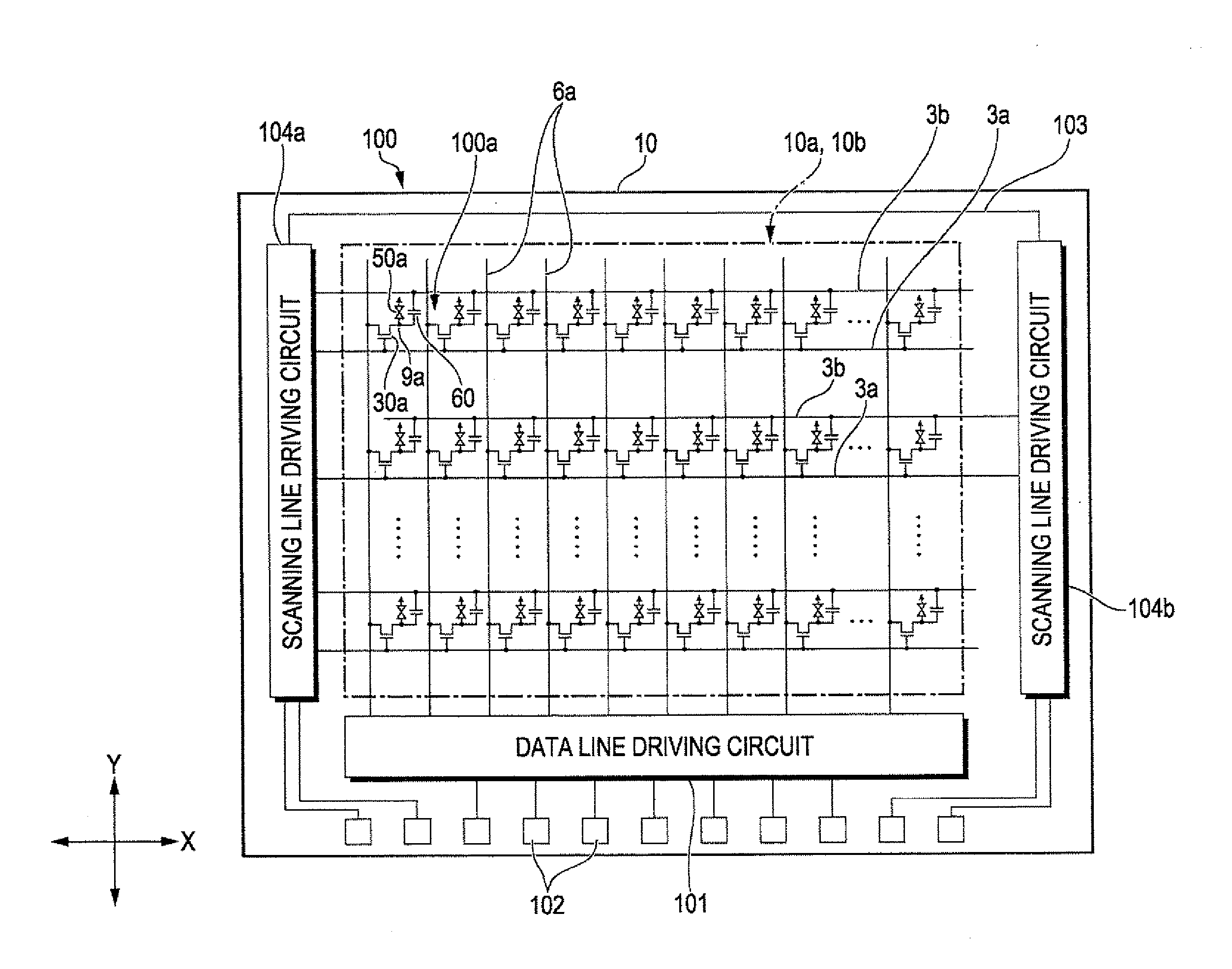
[0053]FIG. 1 is a block diagram showing the electrical configuration of an electrooptical device (liquid crystal device) according to Embodiment 1 of the invention. As shown in FIG. 1, the electro-optical device 100 according to this embodiment is a liquid crystal device. On a component substrate 10 of the electro-optical device 100, a plurality of pixels 100a is formed in positions corresponding to intersections of a plurality of scanning lines 3a (first signal lines) and a plurality of data lines 6a (second signal lines) that extend in directions x and y intersecting each other. In addition, on the component substrate 10, a pixel area 10b is configured by an area in which the plurality of pixels 100a is arranged, and the pixel area 10b is used as an image display area 10a for displaying an image in the electro-optical device 100. However, dummy pixels that do not directly contribute to display may be formed along the outer peripheral edge of the pixel area 10b...

modified example of embodiment 1

[0084]According to the above-described Embodiment 1, in the plurality of the unit circuit blocks 4, the configurations and numbers of the unit circuits 40 and the numbers and pitches of the output lines 44 are the same, and the two-dimensional configurations (the two-dimensional sizes and shapes) of the unit circuit blocks 4 are the same. However, depending on the shape of the pixel area 10b, a plurality of types of unit circuit blocks 4 that have different two-dimensional configurations (the two-dimensional sizes and shapes) such as the configurations and numbers of the unit circuits 40 and the numbers and pitches of the output lines 44 are different may be employed.

embodiment 2

[0085]FIG. 7 is a schematic plan view showing disposition of circuit blocks 4x and 4y in an outside area of a pixel area 10b of a component substrate 10 of an electro-optical device 100 according to Embodiment 2 of the invention. In FIG. 7, scanning lines 3a, capacitor lines 3b, and data lines 6a of the pixel area 10b are not shown. The basic configuration of the electro-optical device 100 according to this embodiment is the same as that according to Embodiment 1, and thus, to each common part, a same reference sign is assigned, and a description thereof is omitted here.

[0086]In Embodiment 1, as the unit circuit blocks 4 constituting the circuit blocks 4a, 4b, 4c, and 4d, only one type of the unit circuit blocks that have a same two-dimensional configuration (a two-dimensional size and shape) is used. However, as shown in FIG. 7, two or more types of the unit circuit blocks 4′ and 4″ that have different two-dimensional configurations (the two-dimensional sizes and shapes) may be use...


PUM


Abstract

An electro-optical device includes first and second signal lines that extend in directions for intersecting each other on a component substrate, a pixel area in which a pixel electrode is disposed in correspondence with an intersection of the first and second signal lines, a signal output circuit that is disposed outside the pixel area and outputs a driving signal to the first signal line, and a connection wiring that connects the signal output circuit and the first signal line together. An outer peripheral edge of the pixel area has a curved portion or a bent portion in a portion facing the signal output circuit, and the signal output circuit includes a plurality of circuit blocks, and the circuit blocks are arranged along the curved portion or the bent portion of the portion facing the signal output circuit with deviated between adjacent circuit blocks in the direction of extension of the first signal line and/or the direction of extension of the second signal line.

Description

BACKGROUND[0001]1. Technical Field[0002]The present invention relates to an electro-optical device such as a liquid crystal device, an organic electro luminescence (hereinafter, referred to as an organic EL) device, a plasma display device, an electrophoresis display device, or a device using an electron discharging element.[0003]2. Related Art[0004]As major electro-optical devices, there are liquid crystal devices, organic EL devices, and the like. In the electro-optical devices, a pixel area, in which a plurality of pixels corresponding to intersections of a plurality of scanning lines and a plurality of data lines that extend in directions for intersecting each other is arranged, is disposed on a component substrate. On the outside of the pixel area in the direction of extension of the plurality of scanning lines, a scanning line driving circuit that outputs signals to the scanning lines is disposed. In addition, in the direction of extension of the plurality of data lines, a dat...

Claims


Application Information

Patent Timeline
IPC IPC(8): G09G3/30
CPCG09G3/3225G09G3/3266G09G2300/0408H01L27/3276G09G2300/0465G09G2310/0232G09G2300/0426H10K59/131G02F1/133G09G3/36G09G3/2096G09G3/3275G09G3/3648G09G3/3677G09G3/3688
Inventor ANZAI, KATSUYAKAWADA, HIDEKIMATSUDA, HIROSHIIWASAKI, YUKITADA
Owner JAPAN DISPLAY INC
Why Eureka
Try Eureka